SLVSA73F April 2010 – July 2014 DRV8825
PRODUCTION DATA.
- 1 Features
- 2 Applications
- 3 Description
- 4 Simplified Schematic
- 5 Revision History
- 6 Pin Configuration and Functions
- 7 Specifications
- 8 Detailed Description
- 9 Application and Implementation
- 10Power Supply Recommendations
- 11Layout
- 12Device and Documentation Support
- 13Mechanical, Packaging, and Orderable Information
10 Power Supply Recommendations
The DRV8825 is designed to operate from an input voltage supply (VMx) range between 8.2 and 45 V. Two
0.1-µF ceramic capacitors rated for VMx must be placed as close as possible to the VMA and VMB pins respectively (one on each pin). In addition to the local decoupling caps, additional bulk capacitance is required and must be sized accordingly to the application requirements.
10.1 Bulk Capacitance
Bulk capacitance sizing is an important factor in motor drive system design. It is dependent on a variety of factors including:
- Type of power supply
- Acceptable supply voltage ripple
- Parasitic inductance in the power supply wiring
- Type of motor (brushed DC, brushless DC, stepper)
- Motor startup current
- Motor braking method
The inductance between the power supply and motor drive system will limit the rate current can change from the power supply. If the local bulk capacitance is too small, the system will respond to excessive current demands or dumps from the motor with a change in voltage. You should size the bulk capacitance to meet acceptable voltage ripple levels.
The data sheet generally provides a recommended value but system level testing is required to determine the appropriate sized bulk capacitor.
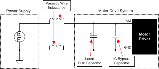 Figure 11. Setup of Motor Drive System With External Power Supply
10.2 Power Supply and Logic Sequencing
There is no specific sequence for powering-up the DRV8825. It is okay for digital input signals to be present before VMx is applied. After VMx is applied to the DRV8825, it begins operation based on the status of the control pins.