SLVK099B March 2022 – September 2023 TPS7H5001-SP , TPS7H5002-SP , TPS7H5003-SP , TPS7H5004-SP
PRODUCTION DATA
- 1
- Abstract
- Trademarks
- 1 Introduction
- 2 Single-Event Effects (SEE)
- 3 Device and Test Board Information
- 4 Irradiation Facility and Setup
- 5 Depth, Range, and LETEFF Calculation
- 6 Test Setup and Procedures
- 7 Destructive Single-Event Effects (DSEE)
- 8 Single-Event Transients (SET)
- 9 Event Rate Calculations
- 10Summary
- A Total Ionizing Dose from SEE Experiments
- B References
- C Revision History
8 Single-Event Transients (SET)
SET are defined as heavy-ion-induced transients upsets on the OUTX, SRX, SS, and Error Amp (while in unity gain) of the TPS7H500x-SP.
Testing was performed at room temperature (no external temperature control applied). The heavy-ions species used for the SET testing were Krypton (84Kr), Silver (109Ag), Praseodymium (141Pr), and Holmium (165 Ho) for an LETEFF = 30 to 75 MeV·cm2/mg. For more details, see Ion LETEFF, Depth, and Range in Silicon. Flux of 7.75 × 10⁴ to 1.65 × 10⁵ ions/cm2·s and a fluence of 9.97 × 10⁶ to 1 × 10⁷ ions/cm2, per run were used for the SET characterization.
SET testing was categorized as:
- VIN = 12 V (nominal)
at FSW = 500 kHz
(All TPS7H500X-SP devices)
. - VIN = 14 V (max) at FSW = 500 kHz.
- VIN = 4 V at FSW = 500 kHz.
- Error amplifier.
- Cross conduction at FSW = 500 kHz.
- VIN = 4 V (min) at FSW = 500 kHz using an external clock with RT = open.
- VIN = 14 V (max) at FSW = 500 kHz using an external clock with RT = open.
- VIN = 4 V (min) 12 V (nominal) and 14 V (max) at FSW = 1 MHz using the internal clock with RT = 90.9 kΩ.
- VIN = 4 V (min) 12 V (nominal) and 14 V (max) at F SW= 2 MHz using the internal clock with RT = 38.3 kΩ.
As the list shows, the only SET case that was repeated for the TPS7H5002/3/4-SP devices was the 12-V nominal at FSW = 500 kHz case. All other SET cases were conducted with the TPS7H5001-SP. This was done due to how closely the TPS7H5002/3/4 devices correlated SET wise to the original TPS7H5001-SP device, specifically having similar number of OUTA and SRB transients and the same found onset.
Cross conduction is a concern in synchronous converter applications due to the possibility of a short circuit during an SET upset. In addition to the hardware X-conduction testing, all recorded upsets during all runs discussed on this report (SEL, SEB, and SET) were verified for such conditions when possible. Using software, cross conduction was verified for:
- OUTA to SRA.
- OUTB to SRB.
- OUTA to OUTB.
The PWM signals were converted to digital levels by comparing the voltage levels of the recorded upset to an VIH = 1.89 V (VIH from the LMG1205 GaN driver was used). If the signals were greater than this voltage, a digital one was returned. Otherwise, a logical 0 was recorded. After the signals were converted into a digital value array, a BITAND was implemented using the desired waveforms. If any logical 1 was present on the resulting response, a cross conduction was said to occur. Not a single upset of this kind was recorded across all upsets and all runs including SEL, SEB, and SET.
Table 8-1 shows waveform size, sample rate, trigger type, value, and signal for all scopes used. For SS, not a single capture was recorded under the conditions used for the data collection. For this reason, the data is not presented in the table.
| Scope Model | Trigger Signal | Trigger Type | Trigger Value | Record Length | Sample Rate |
|---|---|---|---|---|---|
| DPO7104C | OUTA | Pulse-Width (Outside) | ±30% | 500 ns/div or 2 μs/div | 2.5 or 5 GS/s |
| COMP | Window (Outside) | ±10% | |||
| AND Gate (X-Conduction) | Edge-Positive | 2.5 V | |||
| PXIe-5110 | SRB | Pulse-Width (Outside) | ±30% | 4 kS | 100 MS/s |
| PXIe-5162 | SS | Edge/Negative | 0.6 | 100 kS | 2.5 MS/s |
VIN = 12 V (Nominal) at FSW = 500 kHz
For VIN = 12 V and switching frequency of 500 kHz, the results are presented in Table 8-4. The outside-pulse width trigger was set to 30% from the nominal pulse width for both the DPO7104C and the PXIe-5110. Upper-bound cross section at 95% confidence interval and based on SLVK047 are presented in Table 8-3 and Table 8-4. The cross-section plot for this case and Weibull parameter are shown in Figure 8-1 and Table 8-5, respectively. A typical time domain plot for OUTA is shown in Figure 8-2. Since the main concern for a DC-DC converter is the OUTX, (OUTA and OUTB have similar if not equal performance), the OUTA signal was used to characterize the Onset. Due to SRX performing worse behavior than OUTX, the onset was not found during testing. To accurately determine the onset for SRX, a Weibull fit plot was created. Conditions and the Weibull fit plot for SRB are shown below with the remaining 12-V 500-kHz results.
For the TPS7H5002/3-SP SRA instead of SRB was monitored.
| Run Number | Device | Unit Number | Ion | LETEFF (MeV·cm2/mg) | Flux (ions·cm2/mg) | Fluence (Number of Ions) | Number of DPO7104C ≥ 30% (OUTA | Number of PXIe-5110 ≥ 30% (SRB) |
|---|---|---|---|---|---|---|---|---|
| 11 | TPS7H5001 | 3 | 165Ho | 75 | 1.20 × 10⁵ | 1 × 10⁷ | 114 | N/A |
| 12 | TPS7H5001 | 4 | 141Pr | 75 | 1.07 × 10⁵ | 1 × 10⁷ | 96 | 464 |
| 13 | TPS7H5001 | 4 | 141Pr | 65 | 1.06 × 10⁵ | 9.99 × 10⁶ | 91 | 409 |
| 14 | TPS7H5001 | 2 | 141Pr | 75 | 9.51 × 10⁴ | 1 × 10⁷ | 108 | 532 |
| 15 | TPS7H5001 | 2 | 141Pr | 65 | 1.03 × 10⁵ | 1 × 10⁷ | 79 | 414 |
| 16 | TPS7H5001 | 3 | 109Ag | 48 | 1.22 × 10⁵ | 9.98 × 10⁶ | 30 | N/A |
| 17 | TPS7H5001 | 3 | 109Ag | 48 | 1.39 × 10⁵ | 9.96 × 10⁶ | 9 | N/A |
| 18 | TPS7H5001 | 3 | 109Ag | 48 | 1.29 × 10⁵ | 9.98 × 10⁶ | N/A | 300 |
| 19 | TPS7H5001 | 4 | 109Ag | 48 | 8.27 × 10⁴ | 1 × 10⁷ | 12 | 286 |
| 20 | TPS7H5001 | 7 | 84Kr | 40 | 1.36 × 10⁵ | 9.95 × 10⁶ | 3 | 273 |
| 21 | TPS7H5001 | 7 | 84Kr | 37 | 1.24 × 10⁵ | 9.99 × 10⁶ | 0 | 249 |
| 22 | TPS7H5001 | 7 | 84Kr | 30 | 1.37 × 10⁵ | 9.96 × 10⁶ | 0 | 245 |
| 82 | TPS7H5002 | 9 | 165Ho | 74 | 1.13 × 10⁵ | 1 × 10⁷ | 84 | 577 |
| 83 | TPS7H5003 | 10 | 165Ho | 75 | 1.19 × 10⁵ | 1 × 10⁷ | 96 | 546 |
| 84 | TPS7H5004 | 11 | 165Ho | 75 | 1.14 × 10⁵ | 9.99 × 10⁶ | 104 | N/A |
| 85 | TPS7H5002 | 9 | 84Kr | 30 | 1.12 × 10⁵ | 9.96 × 10⁶ | 0 | 212 |
| 86 | TPS7H5003 | 10 | 84Kr | 30 | 1.06 × 10⁵ | 9.95 × 10⁶ | 0 | 216 |
| 87 | TPS7H5004 | 11 | 84Kr | 30 | 1.05 × 10⁵ | 1 × 10⁷ | 0 | N/A |
| LETEFF (MeV·cm2/mg) | Number of Upsets | Upper Bound X-Section (cm2) |
|---|---|---|
| 30 | 0 | 3.70 × 10⁻⁷ |
| 37 | 0 | 3.69 × 10⁻⁷ |
| 40 | 3 | 8.81 × 10⁻⁷ |
| 48 | 51 | 2.24 × 10⁻⁶ |
| 65 | 170 | 9.88 × 10⁻⁶ |
| 75 | 318 | 1.18 × 10⁻⁵ |
| LETEFF (MeV·cm2/mg) | Number of Upsets | Upper Bound X-Section (cm2) |
|---|---|---|
| 30 | 245 | 2.79 × 10⁻⁵ |
| 37 | 249 | 2.82 × 10⁻⁵ |
| 40 | 273 | 3.09 × 10⁻⁵ |
| 48 | 586 | 3.18 × 10⁻⁵ |
| 65 | 823 | 4.41 × 10⁻⁵ |
| 75 | 996 | 5.30 × 10⁻⁵ |
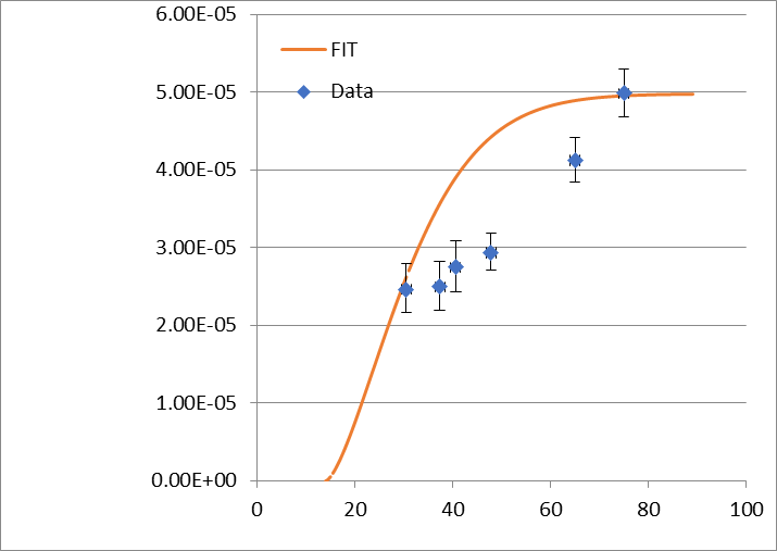
Upper and lower bound were calculated to 95% confidence. Weibull fit was done for the mean value.
Figure 8-1 Cross Section and Weibull Fit for SRB at VIN = 12 V and FSW= 500 kHz| Parameter | Value |
|---|---|
| Upper Bound X-Section | 5.30 × 10⁻⁵ |
| X-Sat | 4.98 × 10⁻⁵ |
| Onset | 14 |
| W | 20 |
| s | 1.5 |
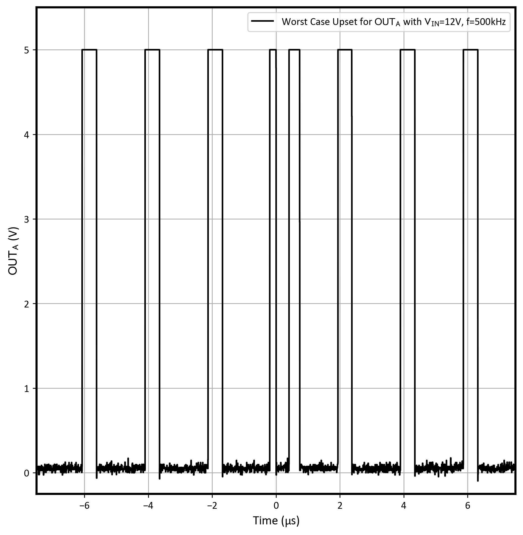 Figure 8-2 Worst Case OUTA Time Domain
Upset (Run Number 14)
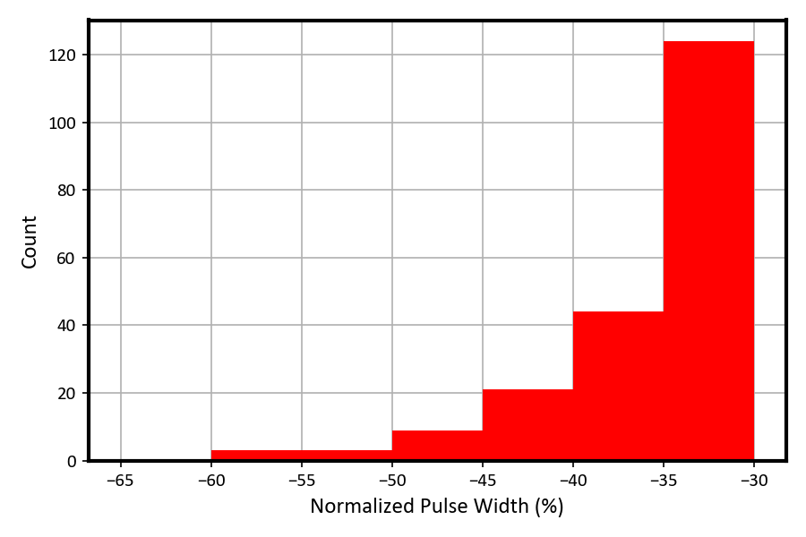 Figure 8-3 OUTA Normalized Percentage
Pulse Width Deviation During Trigger
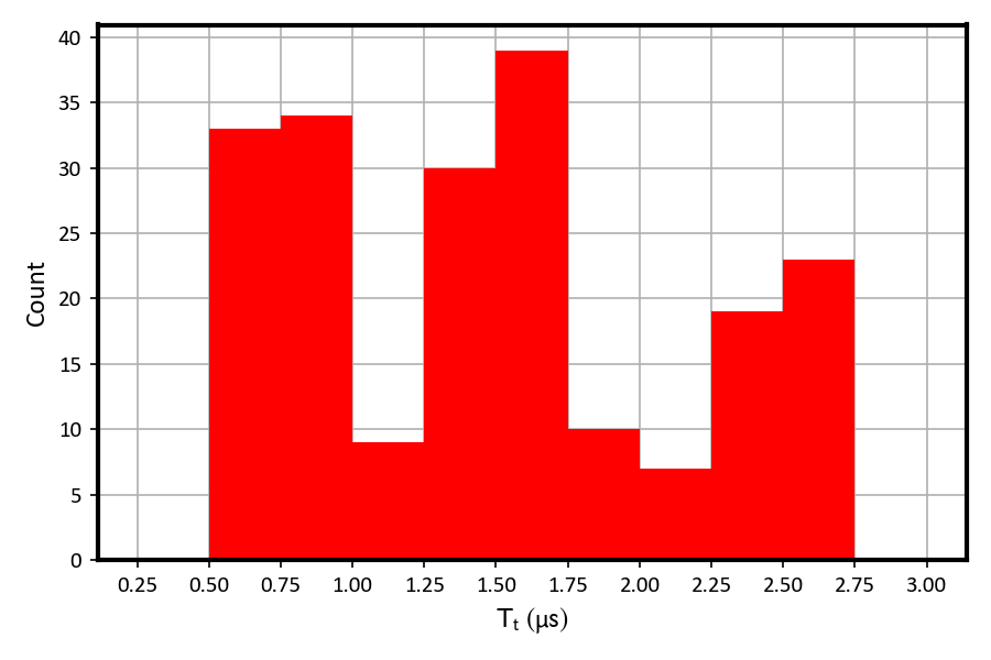 Figure 8-4 OUTA Duration of Triggers
(µs)
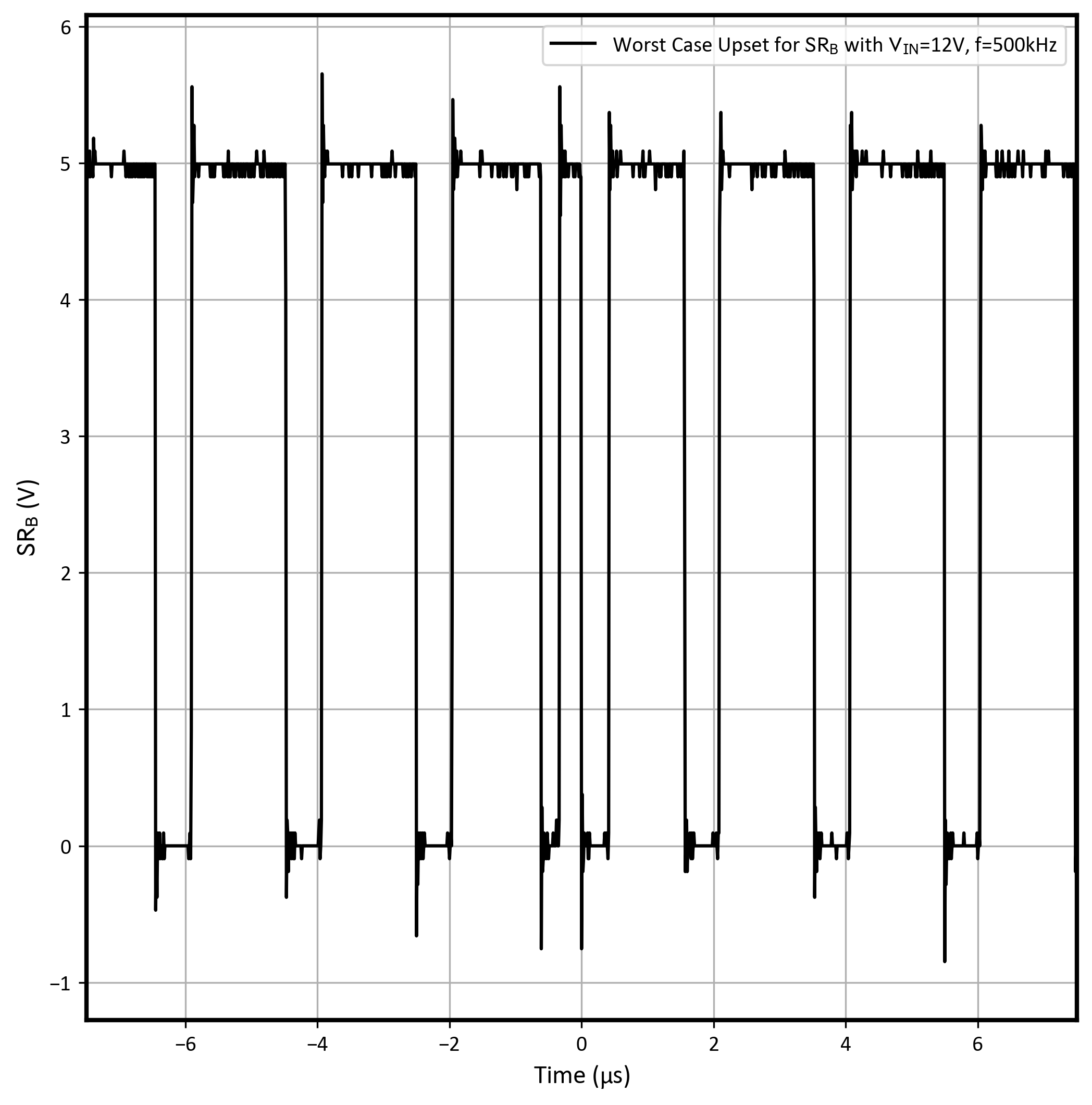 Figure 8-5 Worst Case SRB Time Domain
Upset (Run Number 14)
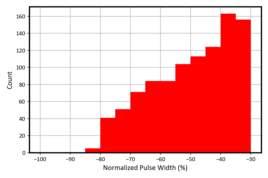 Figure 8-6 SRB Normalized Percentage
Pulse Width Deviation During Trigger
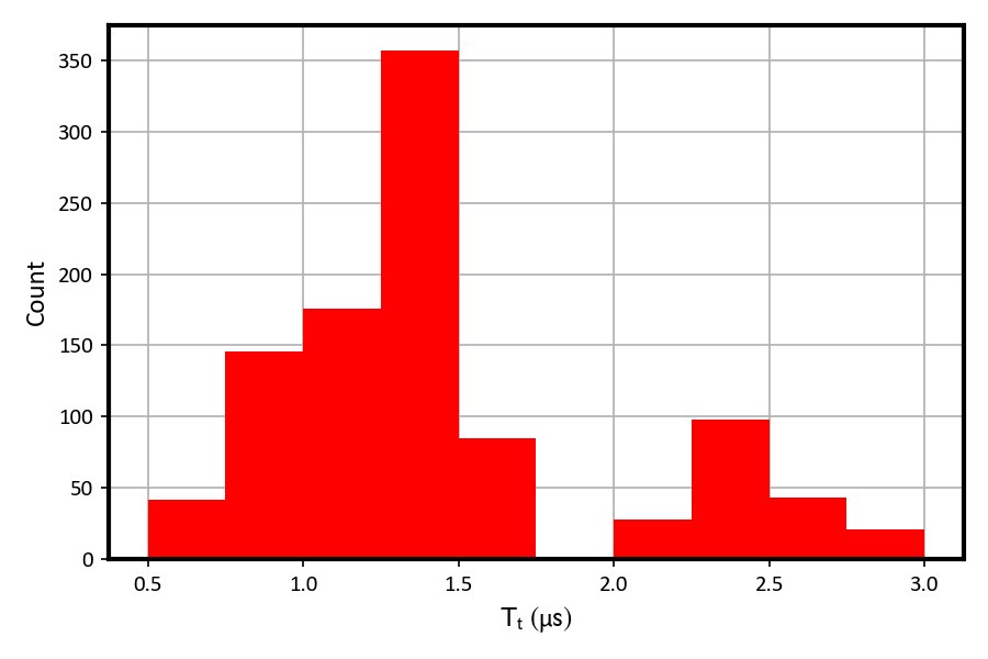 Figure 8-7 SRB Duration of Triggers
(µs)
Figure 8-7 SRB Duration of Triggers
(µs)VIN= 14 V (Maximum) at FSW= 500 kHz
| Run Number | Unit Number | Ion | LETEFF (MeV·cm2/mg) | FLUX (ions·cm2/mg) | Fluence (Number of Ions) | Number DPO7104C ≥ 30% (OUTA) | Number PXIe-5110 ≥ 30% (SRB) |
|---|---|---|---|---|---|---|---|
| 23 | 4 | 141Pr | 75 | 8.85 × 10⁴ | 9.97 × 10⁶ | 100 | 496 |
| 24 | 4 | 141Pr | 75 | 1.03 × 10⁵ | 9.99 × 10⁶ | 93 | 494 |
| 25 | 4 | 141Pr | 65 | 1.11 × 10⁵ | 9.97 × 10⁶ | 61 | 400 |
| 26 | 2 | 141Pr | 75 | 1.09 × 10⁵ | 1.00 × 10⁷ | 120 | 488 |
| 27 | 2 | 141Pr | 65 | 1.04 × 10⁵ | 1.00 × 10⁷ | 80 | 372 |
| 28 | 4 | 109Ag | 48 | 8.19 × 10⁴ | 1.00 × 10⁷ | 13 | 290 |
| 29 | 7 | 84Kr | 37 | 1.17× 10⁵ | 1.00 × 10⁷ | 1 | 232 |
VIN=4-V (Min) at FSW = 500 kHz
| Run Number | Unit Number | Ion | LETEFF (MeV·cm2/mg) |
Flux (ions·cm2/mg) |
Fluence (Number of Ions) |
Number of DPO7104C ≥ 30% (OUTA) | Number of PXIe-5110 ≥ 30% (SRB) |
|---|---|---|---|---|---|---|---|
| 30 | 4 | 141Pr | 75 | 1.09 × 10⁵ | 1.00 × 10⁷ | 111 | 617 |
| 31 | 4 | 141Pr | 65 | 1.19 × 10⁵ | 1.00 × 10⁷ | 25 | 424 |
| 32 | 4 | 141Pr | 65 | 1.09 × 10⁵ | 1.00 × 10⁷ | 112 | 479 |
| 33 | 4 | 141Pr | 65 | 1.15 × 10⁵ | 9.98 × 10⁶ | 76 | 451 |
| 34 | 2 | 141Pr | 75 | 7.66 × 10⁴ | 1.00 × 10⁷ | 109 | 577 |
| 35 | 2 | 141Pr | 65 | 1.00 × 10⁵ | 1.00 × 10⁷ | 79 | 474 |
| 36 | 4 | 109Ag | 48 | 9.38 × 10⁴ | 1.00 × 10⁷ | 22 | 306 |
| 37 | 7 | 84Kr | 37 | 1.35 × 10⁵ | 9.98 × 10⁶ | 0 | 210 |
Error Amp in Unity Gain
Time Domain Plots for the COMP voltage and Normalized max Value for each upset is shown on Nominal Trigger on COMP Run Number 43 VIN = 12 V
| Run Number | Unit Number | VIN (V) | Ion | LETEFF (MeV·cm2/mg) | Flux (ions·cm2/mg) | Fluence (Number of Ions) | Number of Upsets COMP ≥ |10|% |
|---|---|---|---|---|---|---|---|
| 38 | 8 | 14 | 141Pr | 75 | 1.53 × 10⁵ | 1.00 × 10⁷ | 11 |
| 39 | 8 | 12 | 141Pr | 75 | 1.65 × 10⁵ | 1.00 × 10⁷ | 0 |
| 40 | 8 | 4 | 141Pr | 75 | 1.51 × 10⁵ | 1.00 × 10⁷ | 0 |
| 41 | 8 | 4 | 141Pr | 65 | 1.30 × 10⁵ | 1.00 × 10⁷ | 0 |
| 42 | 8 | 12 | 141Pr | 65 | 1.41 × 10⁵ | 1.00 × 10⁷ | 0 |
| 43 | 8 | 14 | 141Pr | 65 | 1.32 × 10⁵ | 1.00 × 10⁷ | 32 |
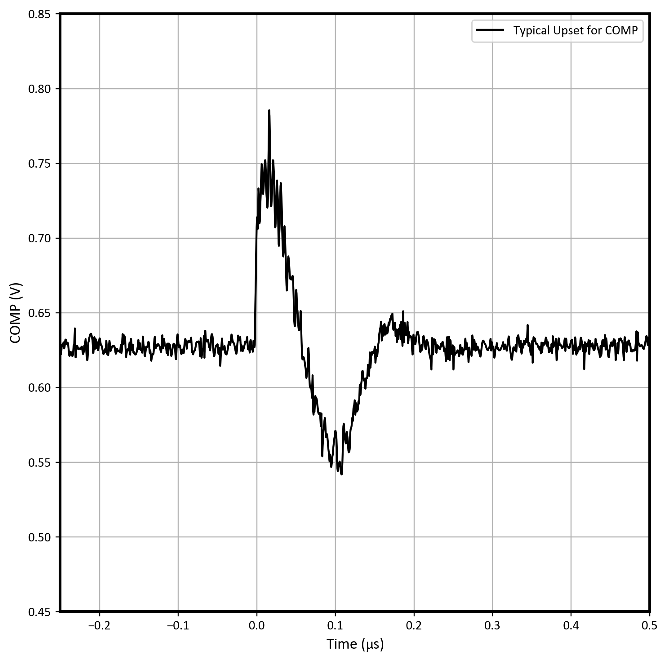 Figure 8-8 Nominal Trigger on COMP Run
Number 43 VIN = 12 V
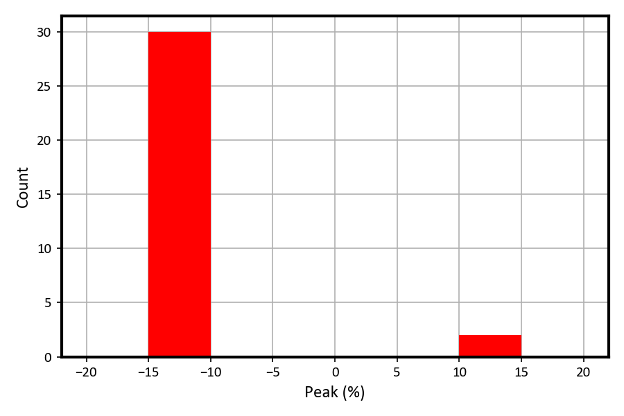 Figure 8-9 Comp Peak Percentage Deviation
from Nominal of Triggers
Figure 8-9 Comp Peak Percentage Deviation
from Nominal of TriggersCross-Conduction (Using Hardware) at FSW = 500 kHz
For cross conduction using hardware an AND Gate (model: SN74AHCT1G08DCKR) was used. IN1 was set as OUTA and IN2 was used as SRA. The output of the AND gate was connected to the CH number 1 of the DPO7104C with an edge trigger at 2.5 V. Not a single trigger was capture indicating that the TPS7H500x-SP is cross-conduction free at the conditions tested and presented here. As mention in the SET introduction, all recorded upset were also verified for the cross conduction in software and not a single cross conduction upset was recorded.
| Run Number | Unit Number | VIN (V) | Ion | LETEFF (MeV·cm2/mg) | Flux (ions·cm2/mg) | Fluence (Number of Ions) | DPO7104C Number Of Upsets |
|---|---|---|---|---|---|---|---|
| 44 | 3 | 4 | 141Pr | 75 | 1.20 × 10⁵ | 9.97 × 10⁶ | 0 |
| 45 | 3 | 12 | 141Pr | 75 | 1.24 × 10⁵ | 9.98 × 10⁶ | 0 |
| 46 | 3 | 14 | 141Pr | 75 | 1.23 × 10⁵ | 1.00 × 10⁷ | 0 |
FSW = 500 kHz using an External Clock with RT = Open
| Run Number | Unit Number | VIN (V) | Ion | LETEFF (MeV·cm2/mg) | Flux (ions·cm2/mg) | Fluence (Number of Ions) | Number DPO7104C ≥ 30% (OUTA) | Number PXIe-5110 ≥ 30% (SRB) |
|---|---|---|---|---|---|---|---|---|
| 47 | 2 | 4 | 141Pr | 75 | 1.17 × 10⁵ | 1.00 × 10⁷ | 23 | 51 |
| 48 | 2 | 12 | 141Pr | 75 | 1.25 × 10⁵ | 1.00 × 10⁷ | 22 | 28 |
| 49 | 2 | 14 | 141Pr | 75 | 1.19 × 10⁵ | 1.00 × 10⁷ | 1 | 8 |
| 50 | 2 | 4 | 141Pr | 65 | 1.07 × 10⁵ | 1.00 × 10⁷ | 1 | 1 |
| 51 | 2 | 12 | 141Pr | 65 | 1.21 × 10⁵ | 1.00 × 10⁷ | 1 | 2 |
| 52 | 2 | 14 | 141Pr | 65 | 1.18 × 10⁵ | 1.00 × 10⁷ | 1 | 3 |
| 53 | 2 | 4 | 109Ag | 48 | 1.00 × 10⁵ | 9.98 × 10⁶ | 0 | 0 |
| 54 | 2 | 12 | 109Ag | 48 | 8.96 × 10⁴ | 1.00 × 10⁷ | 0 | 0 |
| 55 | 2 | 14 | 109Ag | 48 | 9.30 × 10⁴ | 1.00 × 10⁷ | 0 | 0 |
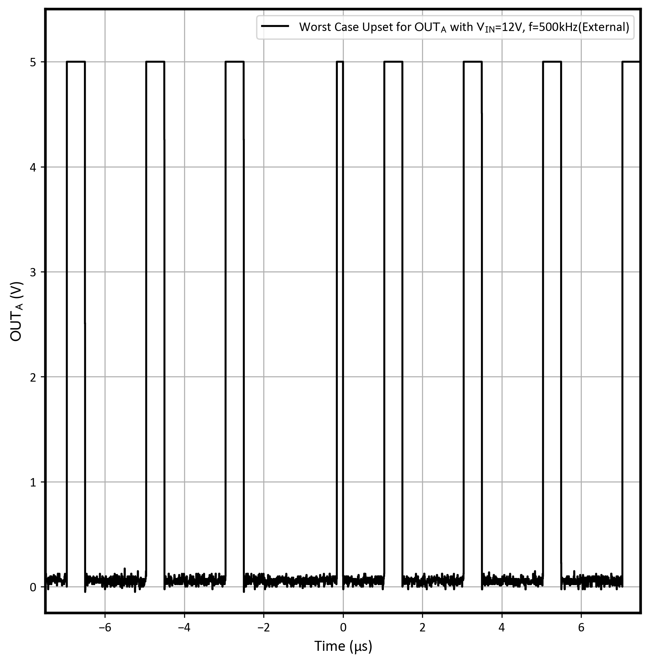 Figure 8-10 Worst Case OUTA Time Domain
Upset (Run Number 48)
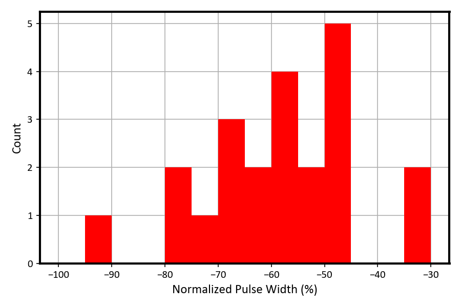 Figure 8-11 OUTA Normalized Percentage
Pulse Width Deviation During Trigger With External Clock
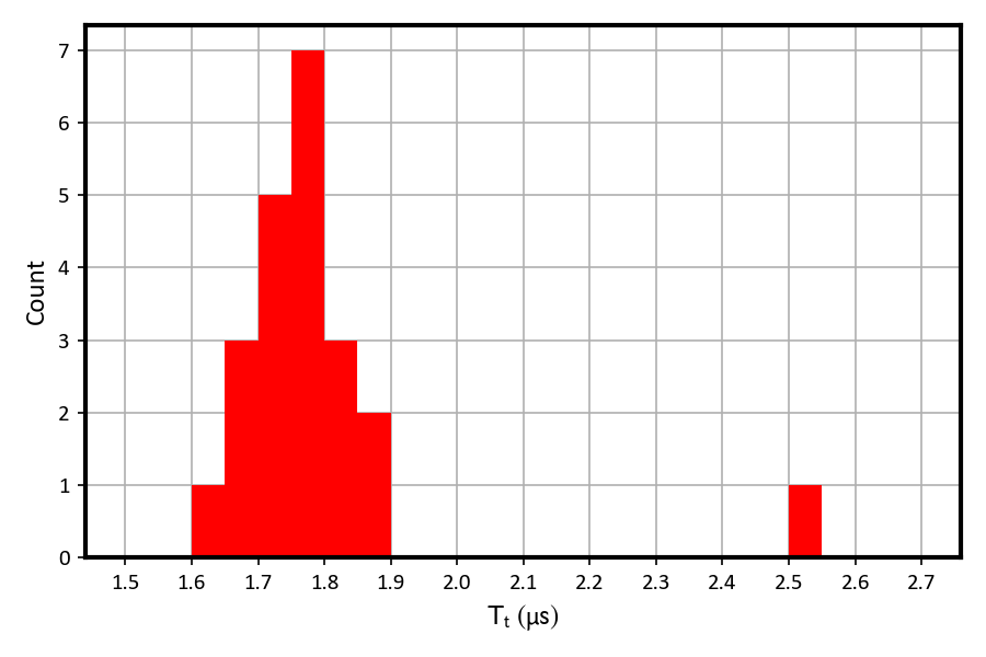 Figure 8-12 OUTA Duration of Triggers (µs)
With External Clock
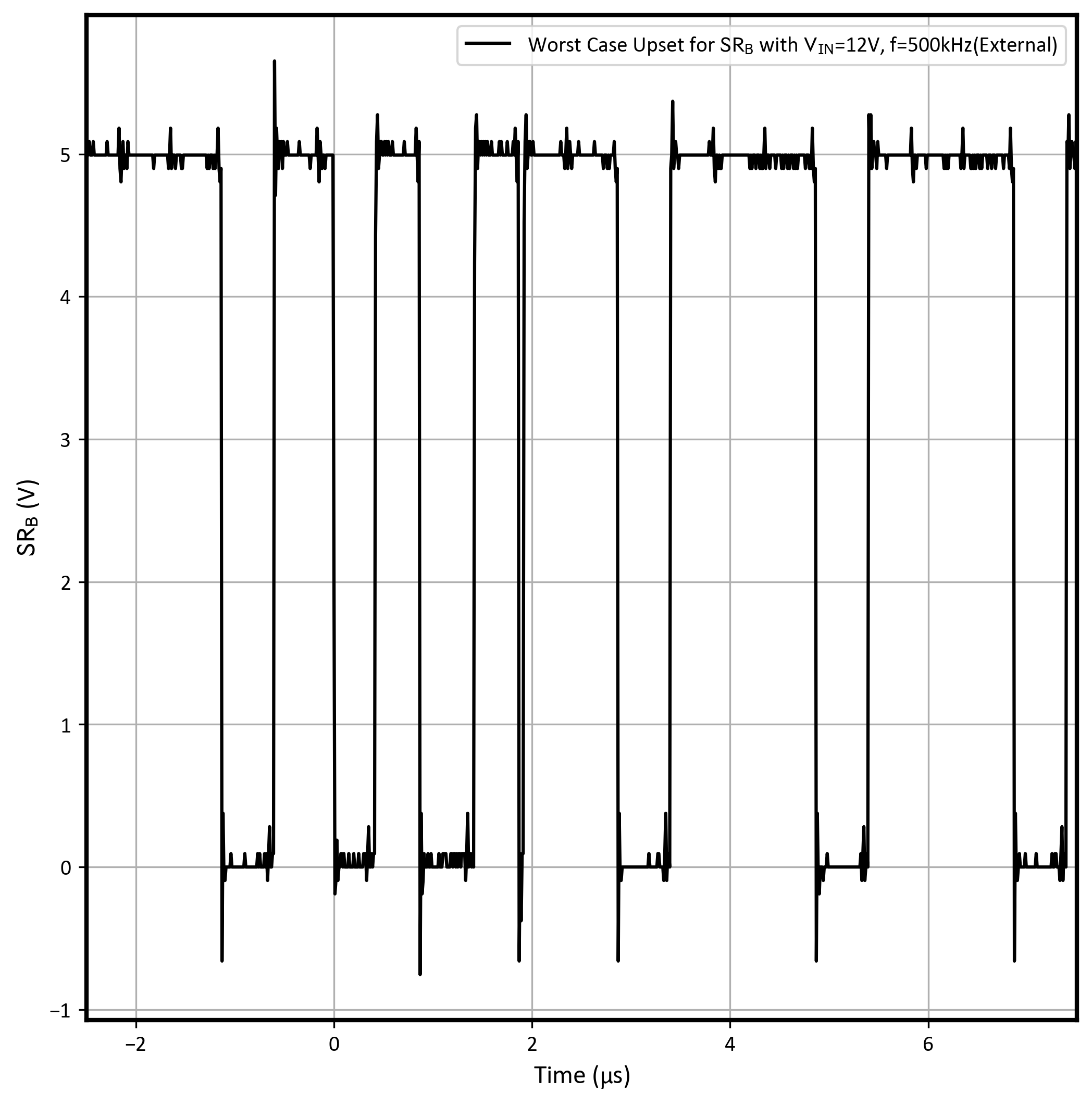 Figure 8-13 Worst Case SRB Time Domain
Upset (Run Number 48)
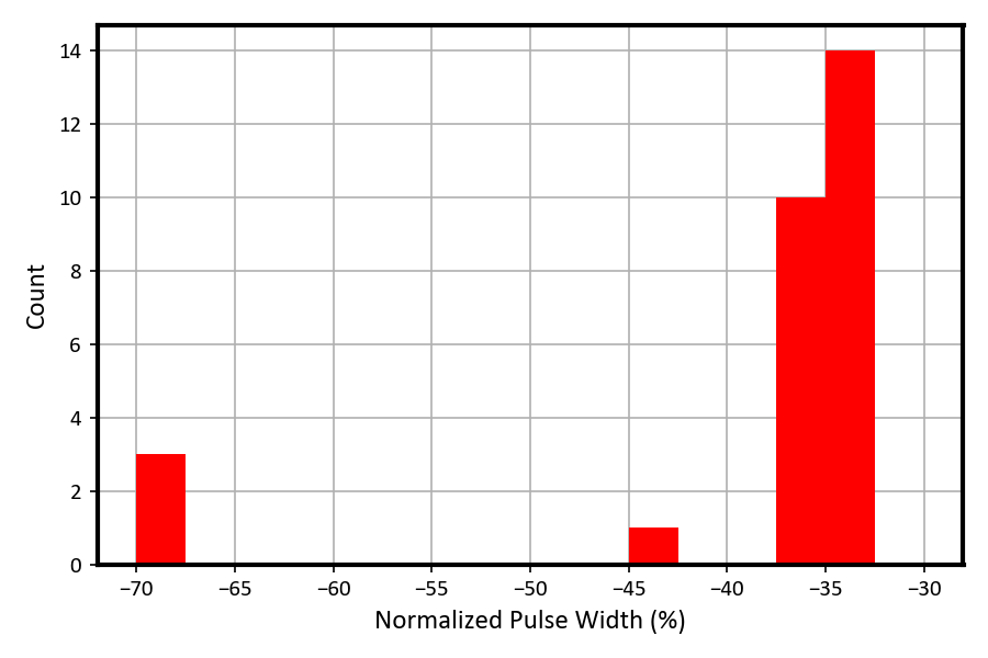 Figure 8-14 SRB Normalized Percentage
Pulse Width Deviation During Trigger With External Clock
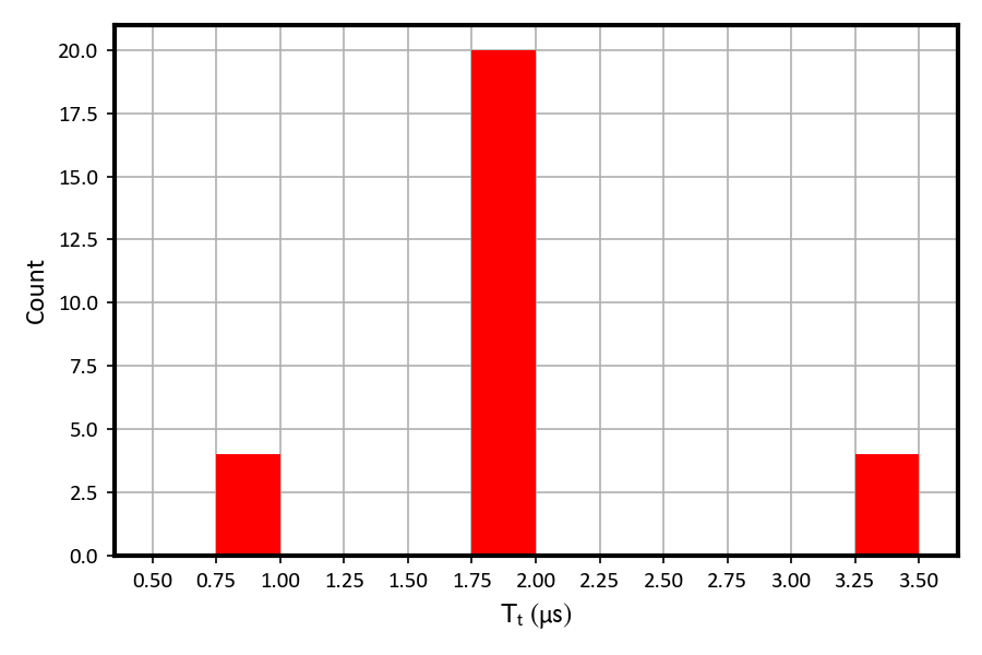 Figure 8-15 SRB Duration of Triggers (µs)
With External Clock
Figure 8-15 SRB Duration of Triggers (µs)
With External ClockFSW = 1 MHz Using an Internal Clock with RT = 90.9 kΩ
| Run Number | Unit Number | VIN (V) | Ion | LETEFF (MeV·cm2/mg) | Flux (ions·cm2/mg) | Fluence (Number of Ions) | Number DPO7104C ≥ 30% (OUTA) | Number PXI 5110 ≥ 30% (SRB) |
|---|---|---|---|---|---|---|---|---|
| 56 | 5 | 4 | 141Pr | 75 | 8.52 × 10⁴ | 1.00 × 10⁷ | 101 | 443 |
| 57 | 5 | 12 | 141Pr | 75 | 8.29 × 10⁴ | 9.99 × 10⁶ | 78 | 422 |
| 58 | 5 | 14 | 141Pr | 75 | 8.85 × 10⁴ | 9.98 × 10⁶ | 67 | 402 |
| 59 | 5 | 4 | 141Pr | 65 | 8.42 × 10⁴ | 1.01 × 10⁷ | 53 | 381 |
| 60 | 5 | 12 | 141Pr | 65 | 8.99 × 10⁴ | 9.98 × 10⁶ | 46 | 328 |
| 61 | 5 | 14 | 141Pr | 65 | 1.00 × 10⁵ | 1.00 × 10⁷ | 55 | 342 |
| 62 | 5 | 4 | 109Ag | 48 | 9.72 × 10⁴ | 9.97 × 10⁶ | 5 | 273 |
| 63 | 5 | 12 | 109Ag | 48 | 9.70 × 10⁴ | 9.99 × 10⁶ | 1 | 260 |
| 64 | 5 | 14 | 109Ag | 48 | 8.28 × 10⁴ | 1.00 × 10⁷ | 1 | 247 |
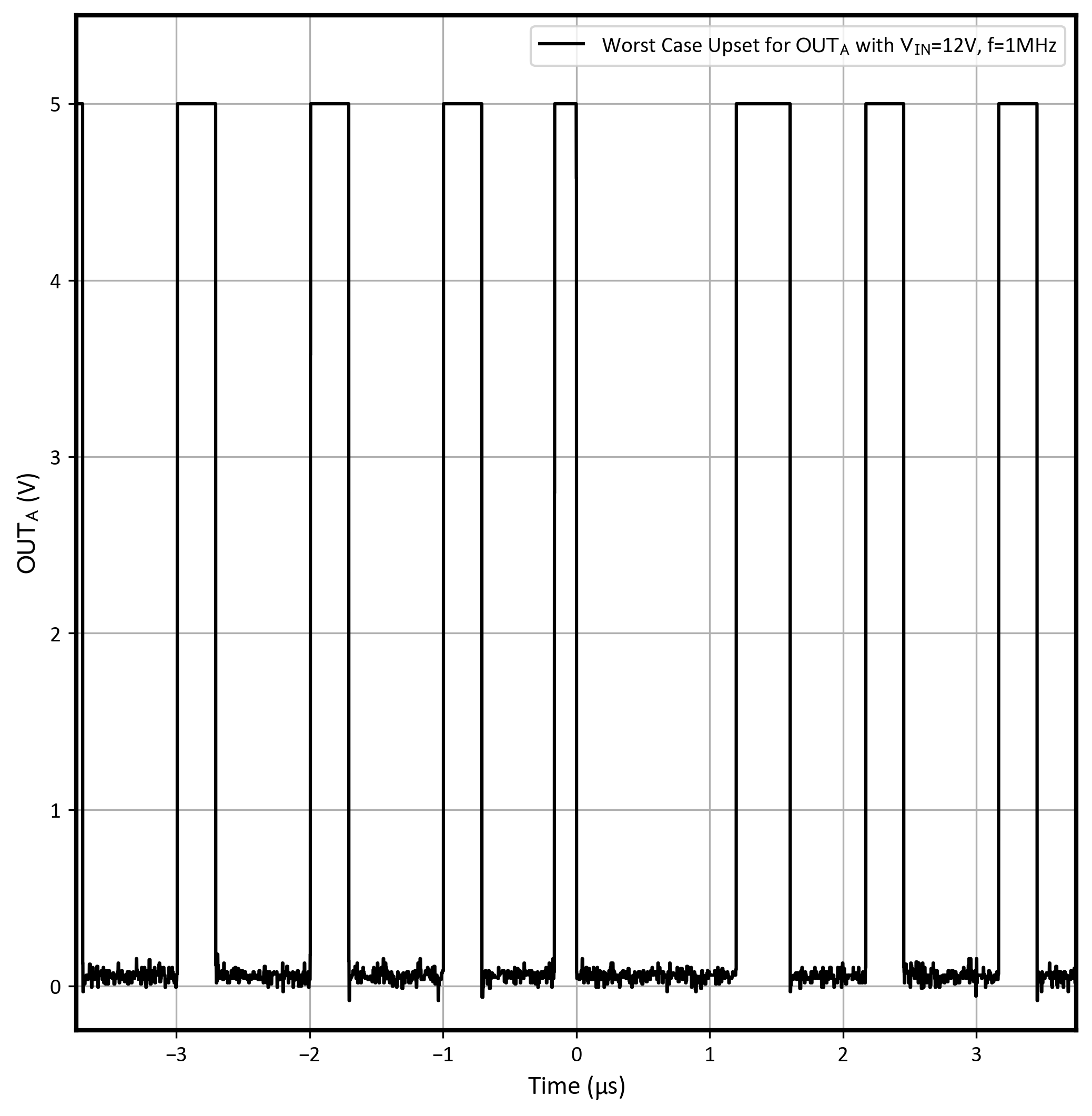 Figure 8-16 Worst Case OUTA Time Domain
Upset (Run Number 57)
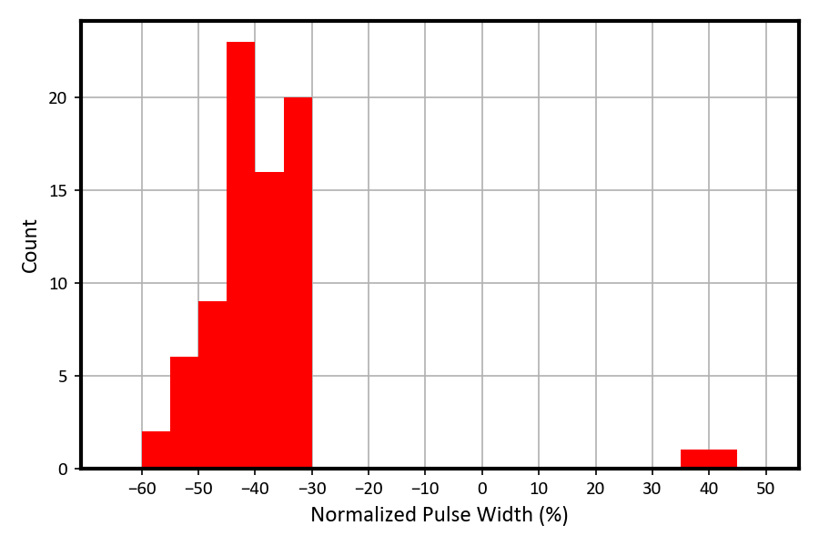 Figure 8-17 OUTA Normalized Percentage
Pulse Width Deviation During Trigger With 1-MHz Internal Clock
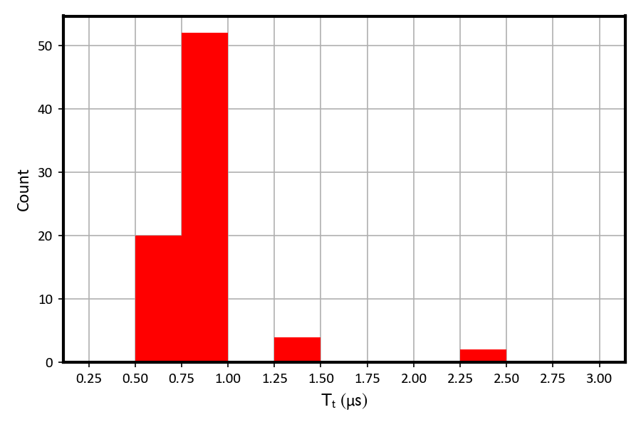 Figure 8-18 OUTA Duration of Triggers (µs)
With 1-MHz Internal Clock
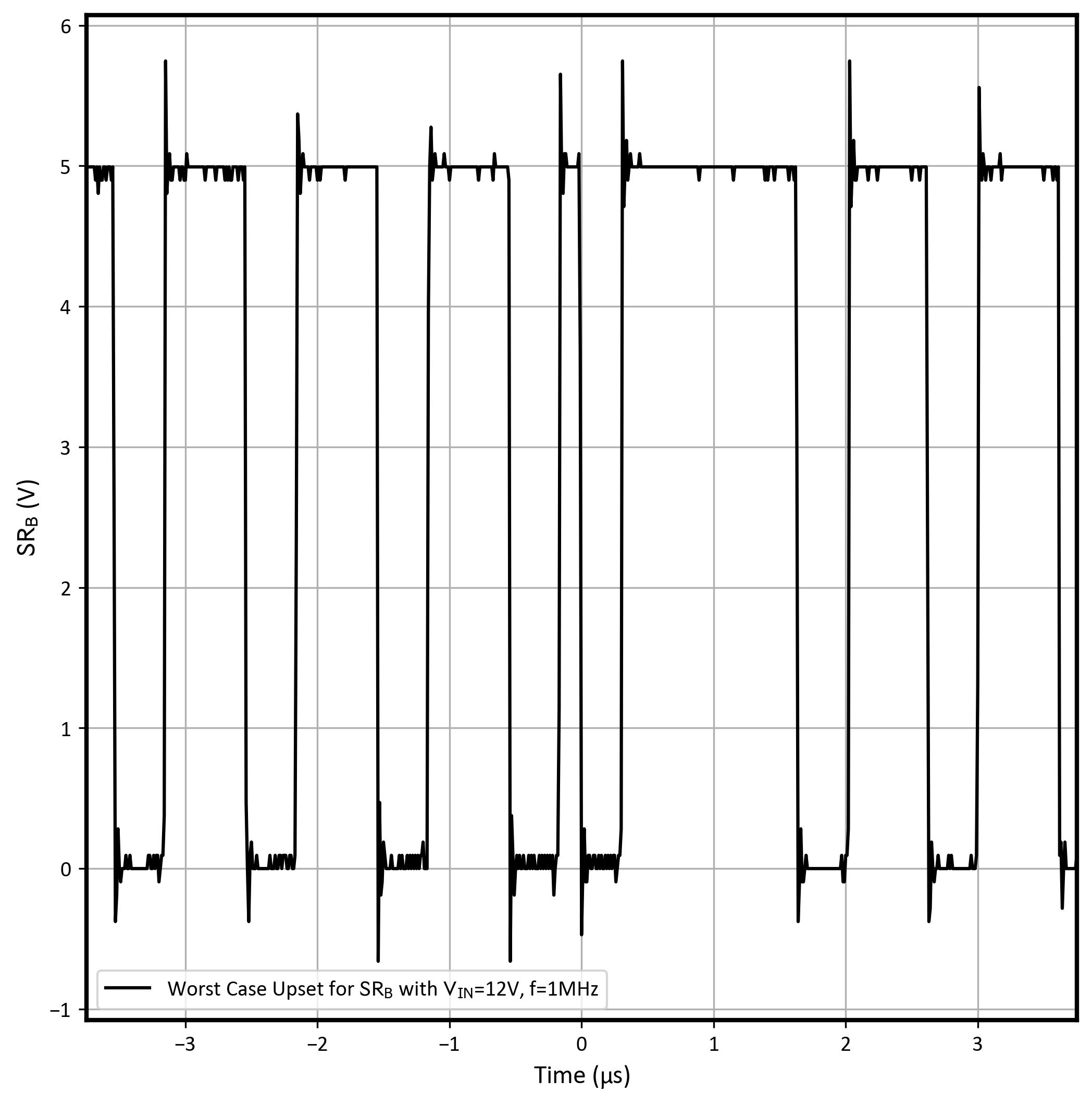 Figure 8-19 Worst Case SRB Time Domain
Upset (Run Number 57)
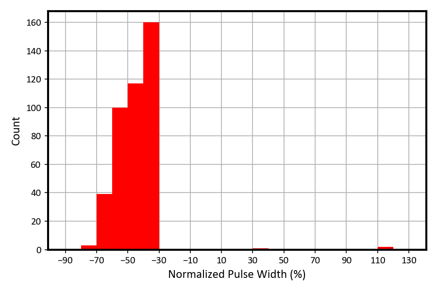 Figure 8-20 SRB Normalized Percentage
Pulse Width Deviation During Trigger With 1-MHz Internal Clock
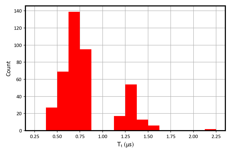 Figure 8-21 SRB Duration of Triggers (µs)
With 1MHz Internal Clock
Figure 8-21 SRB Duration of Triggers (µs)
With 1MHz Internal ClockFSW = 2 MHz Using an Internal Clock with RT = 38.3 kΩ
| Run Number | Unit Number | VIN (V) | Ion | LETEFF (MeV·cm2/mg) | Flux (ions·cm2/mg) | Fluence (Number of Ions) | Number of DPO7104C ≥ 30% (OUTA) | Number of PXI 5110 ≥ 30% (SRB) |
|---|---|---|---|---|---|---|---|---|
| 65 | 6 | 4 | 141Pr | 75 | 1.05 × 10⁵ | 9.97 × 10⁶ | 144 | 379 |
| 66 | 6 | 12 | 141Pr | 75 | 9.89 × 10⁴ | 9.99 × 10⁶ | 10 | 299 |
| 67 | 6 | 14 | 141Pr | 75 | 1.02 × 10⁵ | 9.97 × 10⁶ | 11 | 492 |
| 68 | 6 | 12 | 141Pr | 65 | 1.06 × 10⁵ | 1.00 × 10⁷ | 24 | 245 |
| 69 | 6 | 14 | 141Pr | 65 | 1.07 × 10⁵ | 1.00 × 10⁷ | 9 | 260 |
| 70 | 6 | 12 | 141Pr | 65 | 1.03 × 10⁵ | 1.00 × 10⁷ | 12 | 229 |
| 71 | 6 | 12 | 109Ag | 48 | 8.82 × 10⁴ | 1.00 × 10⁷ | 9 | 235 |
| 72 | 6 | 14 | 109Ag | 48 | 8.79 × 10⁴ | 9.98 × 10⁶ | 12 | 534 |
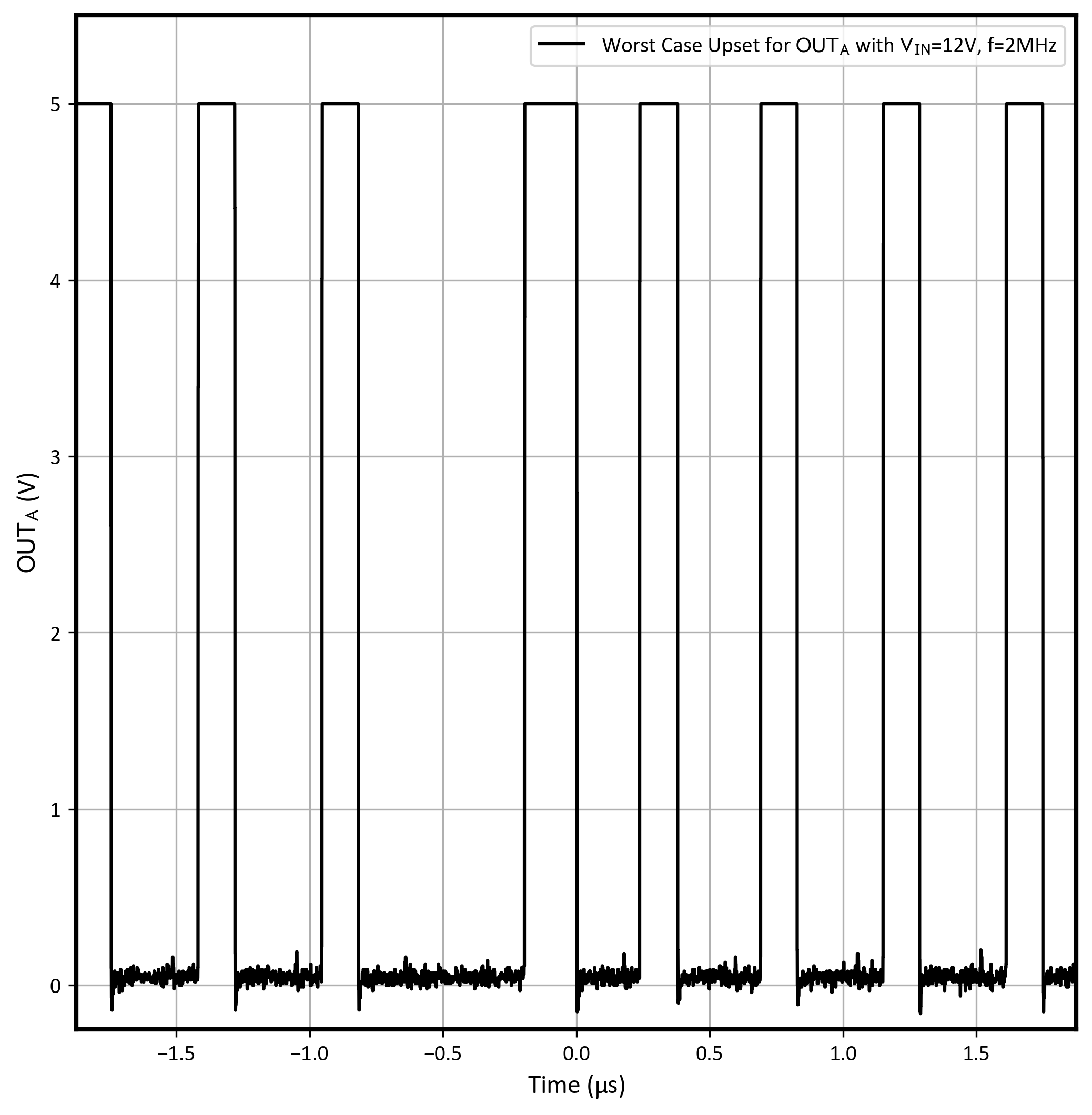 Figure 8-22 Worst Case OUTA Time Domain
Upset (Run Number 66)
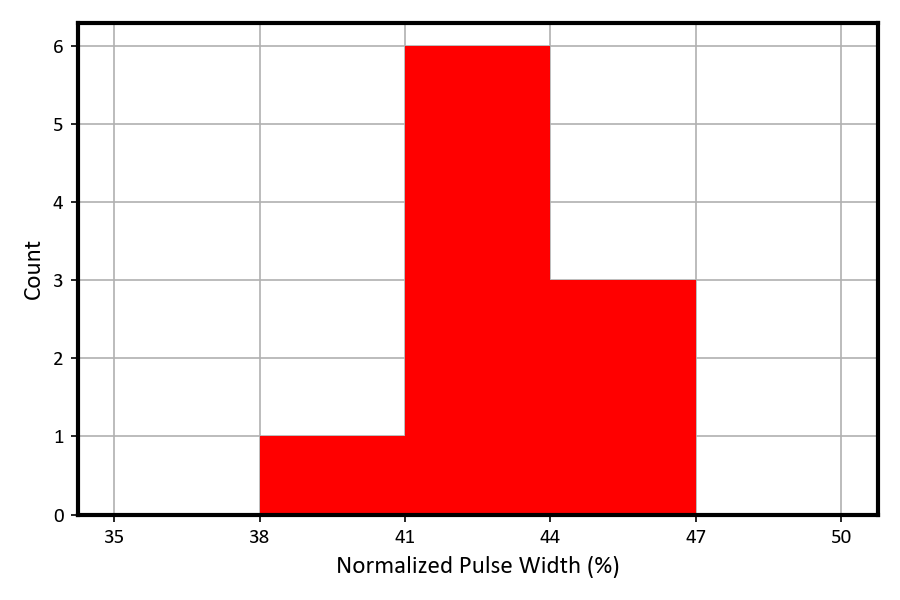 Figure 8-23 OUTA Normalized Percentage
Pulse Width Deviation During Trigger With 2-MHz Internal Clock
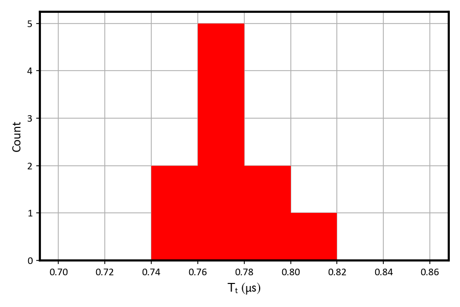 Figure 8-24 OUTA Duration of Triggers (µs)
With 2-MHz Internal Clock
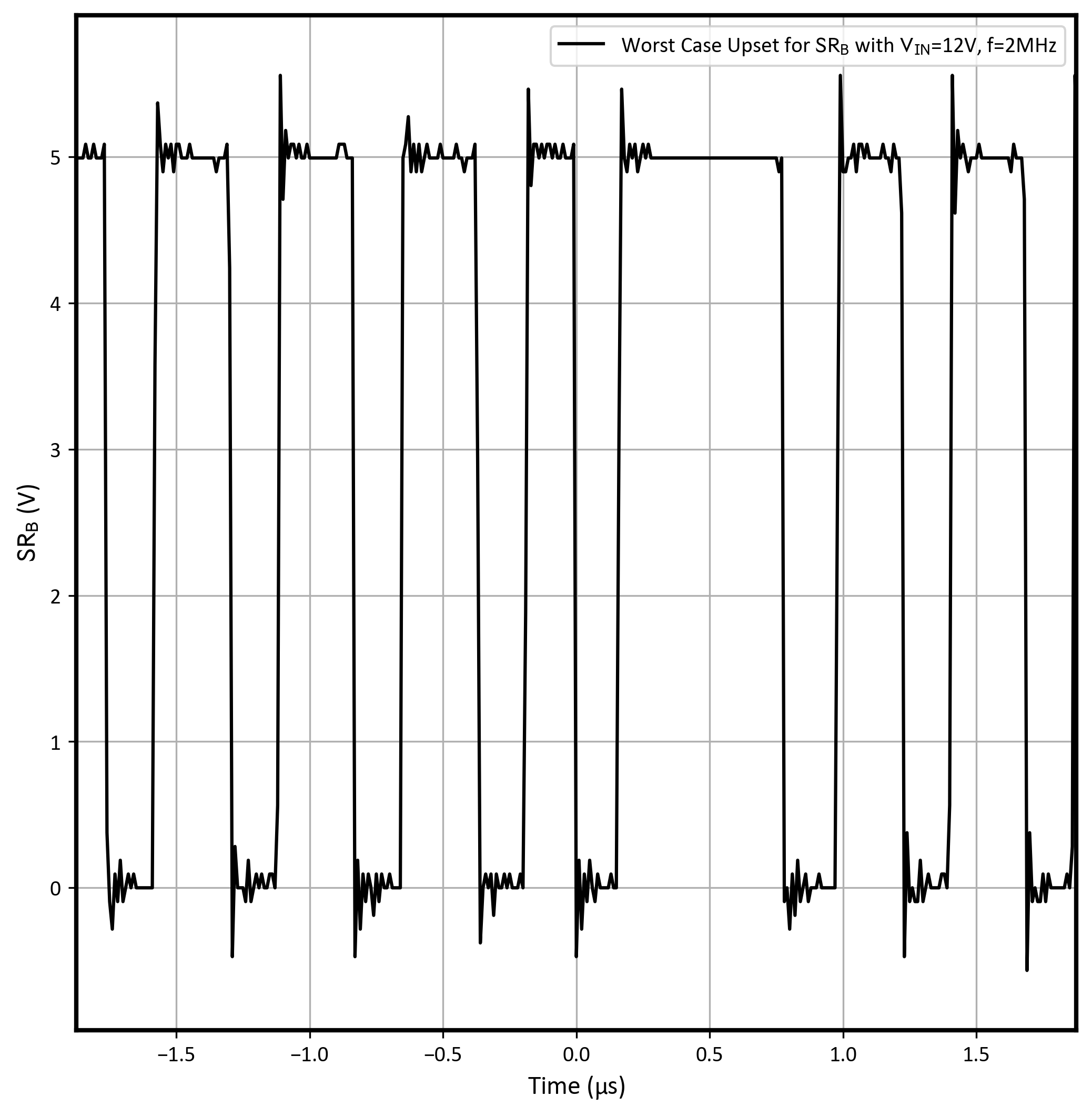 Figure 8-25 Worst Case SRB Time Domain
Upset (Run Number 66)
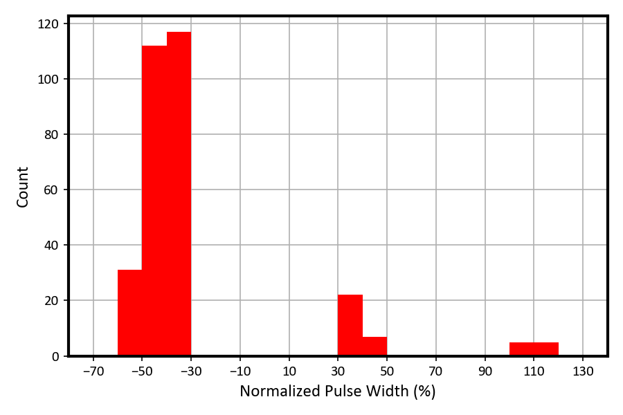 Figure 8-26 SRB Normalized Percentage
Pulse Width Deviation During Trigger With 2-MHz Internal Clock
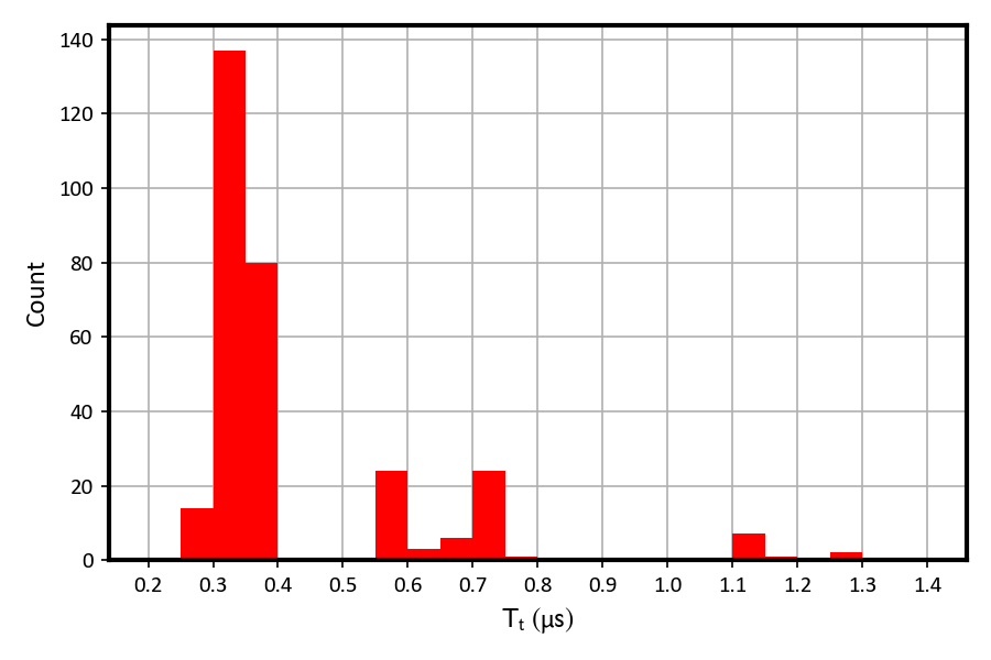 Figure 8-27 SRB Duration of Triggers (µs)
With 2-MHz Internal Clock