SLVK099B March 2022 – September 2023 TPS7H5001-SP , TPS7H5002-SP , TPS7H5003-SP , TPS7H5004-SP
PRODUCTION DATA
- 1
- Abstract
- Trademarks
- 1 Introduction
- 2 Single-Event Effects (SEE)
- 3 Device and Test Board Information
- 4 Irradiation Facility and Setup
- 5 Depth, Range, and LETEFF Calculation
- 6 Test Setup and Procedures
- 7 Destructive Single-Event Effects (DSEE)
- 8 Single-Event Transients (SET)
- 9 Event Rate Calculations
- 10Summary
- A Total Ionizing Dose from SEE Experiments
- B References
- C Revision History
8.1 System Level Implications
To promote a better understanding of the above SET results, this section will look to dissect the results from a system level point of view. One such system level observation is the difference between OUTX and SRX transients in that the OUTX transients have a higher focus than the SRX transients. This is because the primary output of the device has a greater implication on the system as a whole than the synchronous rectifier output does. A second system level observation is that all testing in this report was performed open-loop which is the worst case test-setup for this device. During testing using prototype devices, closed-loop testing was done to validate this idea, the results are presented in the table below.
The testing was conducted using prototype devices. A specially designed push-pull converter evaluation module (EVM) was developed in order to observe the device behavior in a closed-loop DC-DC converter configuration similar to its intended use case. Please refer to Figures 3-4 and 3-5 for an image of the Push-Pull EVM and its schematic.
| LETEFF (MeV·cm2/mg) | FLUX (ions·cm2/mg) | FLUENCE (# ions) | PXIe-5172 Triggering from VOUT at ± ≥ |5|% | PXI 5110 OUTA# ≥ 30% | PXI 5110 OUTA# ≥ 40% | PXI 5110 OUTA# ≥ 50% |
|---|---|---|---|---|---|---|---|
141Pr | 64.7 | 1.10 x 10⁵ | 1.01 x 10⁷ | 0 | 80 | 30 |
|
| 141Pr | 64.7 | 1.30 x 10⁵ | 9.94 x 10⁶ | 0 | 76 | 34 |
|
| 141Pr | 64.7 | 1.04 x 10⁵ | 9.99 x 10⁶ | 0 | 72 | 38 |
|
| 141Pr | 75 | 1.30 x 10⁵ | 3.72 x 10⁶ | 0 | 35 | 17 |
|
| 141Pr | 75 | 1.21 x 10⁵ | 9.96 x 10⁶ | 0 | 99 | 57 |
|
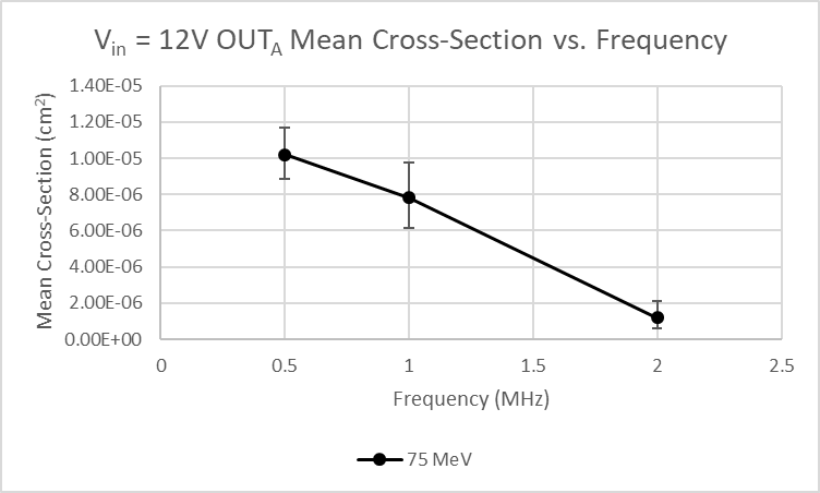
For the open-loop test cases, it is important to demonstrate the difference in device behavior across switching frequency. The SET results of the 500 kHz, 1 MHz, and 2 MHz switching frequencies can best be described by the figure below.
This graph shows that as frequency increases the mean cross-section improves for the nominal VIN case.
 Figure 8-28 Mean Cross-Section vs. Frequency at Nominal VIN
The figure shows that as the frequency increases, so does the performance of the device. The mean cross-section decreases from 500 kHz, to 1 MHz, to 2 MHz which correlates with the expected performance of the device at a system level.