SLVAFE7 September 2022 LM51551
2.1 TI HV Supply Architecture Using SEPIC Topology
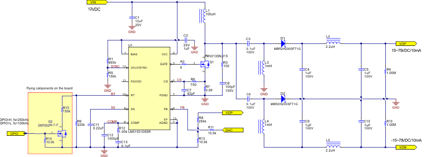
Figure 2-2 shows the schematic of this design. The LM51551 device is used as the controller for the SEPIC circuit. To meet the requirements of height, three uncoupled inductors are used. The switching frequency is set by the RT pin and the output voltage is regulated by the FB pin.
 Figure 2-2 High-Voltage Circuit Design Schematic
For the detailed components selection in SEPIC designs, see the Designing Bipolar High Voltage SEPIC Supply for Ultrasound Smart Probe and AN-1484 Designing A SEPIC Converter application notes. These documents explain how to choose the value of each component based on the design specifications. Also TI has Microsoft®Excel® calculation tools for most DC/DC Converter and Webench, which helps with the power design.