SLVAF70 September 2021 TPS62130
2 Proposed Application Method for Longer Hold-Up Time
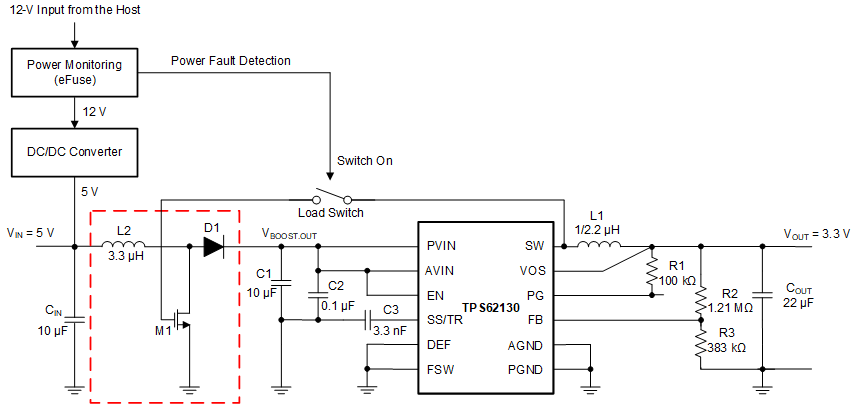
Figure 2-1 shows the proposed application method using the TPS62130 for longer hold-up time. The 5-V input for the TPS62130 comes from the output of another DC/DC converter with 12-V input. By adding L2, D1, and M1, it works as a boost pre-regulator to supply higher voltage to the input of the TPS62130. As Figure 2-1 shows, the advantage of this method is that any additional device to control the boost pre-regulator is not needed, and the gate signal of M1 comes from SW node directly having the same duty ratio in this case. Therefore, no independent PWM control is required for the boost pre-regulator, and this makes the solution more attractive in terms of the total solution cost.

Figure 2-1 Proposed Application Circuit Using Boost Pre-Regulator
Once startup is achieved with the proposed application method, VIN can go down to a couple of volts from 3.3 V while maintaining the output at 3.3 V. Since the output voltage is 3.3 V, VIN never goes below 3.3 V in the typical application of the TPS62130 as Figure 1-1 shows, and it is obviously beneficial to have a longer hold-up time with the proposed method because VIN can go down to around 1 V.
The relationship between the input and the output for the boost converter is:
The on-duty ratio of the boost pre-regulator is calculated as follows:
The relationship between the input and the output for the buck converter can be expressed as follows:
The output of the boost forms the input to the buck. Calculate the on-duty ratio of the buck converter with the TPS62130 using:
Since the gate signal of M1 comes from the SW node directly having the same duty ratio, DON.BOOST should be the same with DON.BUCK.
Therefore, the output voltage of the Boost pre-regulator is determined by:
As Equation 6 shows, this is an interesting result that the output voltage of the boost pre-regulator is being automatically regulated regardless the output load conditions if VIN and VOUT are not changed. Because the input voltage and the output voltage are 5 V and 3.3 V respectively, VBOOST.OUT is regulated to 8.8 V in steady state.
Figure 2-2 shows another application example using a load switch for higher efficiency eliminating the switching loss of the boost pre-regulator. In normal operation, the load switch is turned off to eliminate the switching loss while it is turned on during power fault detection in the system.
The load switch is controlled by the eFuse device, and this eFuse device is designed to protect systems such as enterprise SSDs against sudden power loss event. The eFuse device signals the TPS62130 depending on the system status. The power fault signal remains asserted turning on the load switch until the fault condition is removed, and the load switch is turned off for the normal operation eliminating the switching loss of the boost pre-regulator.

Figure 2-2 Application Example With Load Switch