SLVA934A November 2017 – May 2020 TPS2660
3 Fault Status Monitoring During Reverse Input Supply Connection
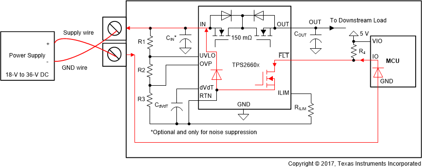
During a faulty reverse input supply connection, the FLTb pin of the TPS2660 can sink current more than its absolute maximum rating under certain power supply sequence. In particular, after a normal power-up and power-down sequence, FLTb pin remains pulled to RTN to indicate brownout faults. Now, if a reverse input supply is applied immediately, the FLTb pin sinks current back into the supply through an external DC/DC converter enable pin or MCU IO pin as it remains pulled to RTN. The current flow path during a reverse input supply connection is indicated in Figure 3.
 Figure 3. Fault Status During Reverse Input Supply Connection
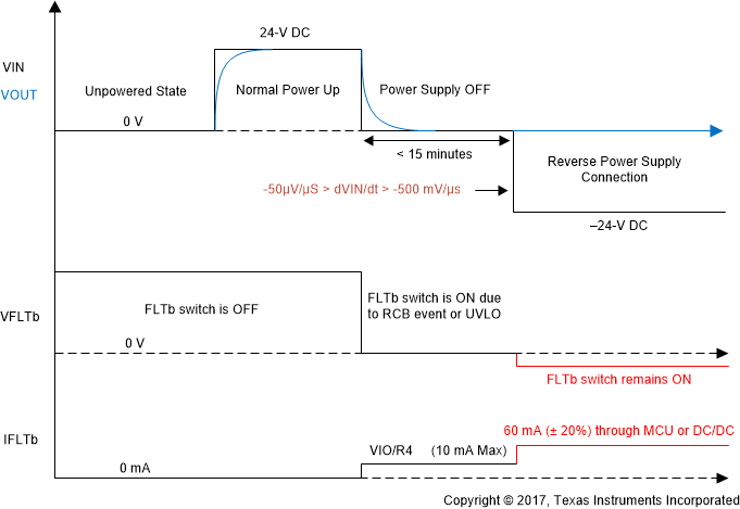
 A specific power supply sequence where FLTb sinks more current is shown in Figure 4 and described below.
- A normal power up is followed by a normal power down.
- The FLTb switch is pulled low to RTN due to a reverse current blocking fault or undervoltage fault.
- A reverse input supply is applied with a slew rate of –50 μV/μs > dVIN/dt > –500 mV/μs within 15 minutes.
- The FLTb switch remains pulled low to RTN and results in a current conduction path shown in Figure 3.
During this reverse input supply sequence, a 60-mA ±20% DC current can flow through the ESD structure of the IO pin of the MCU or the enable pin of the DC/DC converter for a 24-V reverse supply. Table 1 shows the maximum DC current that can flow through the FLTb pin for various power supply voltages. Also note that this DC current does not flow for subsequent reverse supply connections because the FLTb switch is opened after the first reverse supply is removed.
Table 1. Maximum DC Current versus Reverse Supply Voltage
| Parameter | Reverse Supply Voltage | ||
|---|---|---|---|
| –18 V | –24 V | –36 V | |
| Maximum DC current through FLTb | 45 mA ±20% | 60 mA ±20% | 90 mA ±20% |
 Figure 4. Power Supply Sequence Where FLTb Sinks More Current