SLLU332 April 2021 ISOW1044
4 EVM Setup and Operation
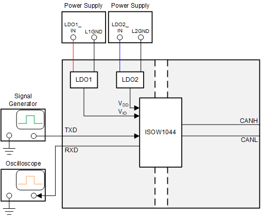
This section describes the typical test setup and operation of the EVM for device evaluation. Figure 4-1 shows a typical test configuration for operating the ISOW1044DFMEVM using two power supplies.
 Figure 4-1 Typical EVM Test Setup
ISOW1044DFMEVM has many DNP resistors which can be populated or unpopulated to setup the EVM to desired operating test conditions. Table 4-1 lists and describes all the possible test configurations that can be acheived by populating jumpers, resistors or other components.
Table 4-1 Jumper, Reseistor and other Test Configurations
| Resistor | Description |
|---|---|
| J3 [5:6] | Populating a jumper on pins 5 and 6 of connector J3 will connect STB pin to VIO and pull it HIGH thereby making the device go to standby mode. Depopulating the jumper or leaving the pins 5 and 6 of J3 OPEN will keep device in active mode. |
| J3 [9:10] | Populating a jumper on pins 9 and 10 of connector J3 will connect EN pin to GND and pull it LOW thereby disabling the DC-DC converter and all the circuit powered by the DC-DC converter. Depopulating the jumper or leaving the pins 5 and 6 of J3 OPEN will keep the DC-DC converter enabled and operating. |
| R1 | It connects LDOs U1, U2 inputs together allowing only one power supply to be used instead of two power supplies. |
| R2, R5, R6, R9 | Sets LDO U2 output voltage to 5 V, 3.3 V, 2.5 V or 1.8 V, respectively. Only one of the four resistors needs to be populated. |
| L1, L2, L5 | Either ferrtie beads (L1 & L5, default) or common-mode choke (L2, ACT45B-510-2P-TL003) can be populated to test the EVM for EMC, especially for radiated emissions. Both ferrite beads and common-mode choke should not be populated at the same time. |
| R10, R3, R14 | Populating R10 bypasses LDO U1 allowing VDD to be powered directly from external power supply. When R10 is populated, R3 and R14 need to be unpopulated to disconnect the LDO. When LDO is not bypassed, the recommended input voltage to LDO should be between 9 V and 12 V. |
| R12, R4, R15 | Populating R12 bypasses LDO U2 allowing VIO to be powered directly from external power supply. When R12 is populated, R4 and R15 need to be unpopulated to disconnect the LDO. When LDO is not bypassed, the recommended input voltage to LDO should be between 9 V and 12 V. |
| R13 | This resistor connects TXD pin to IN pin allowing only one external input signal to be applied to both channels. |
| R21 | It connects oscillator U3 output signal to U4 TXD input allowing EVM to be tested using a test signal without needing any external test signal input. |
| R23 | Default resistance value of 200 kΩ on R23 sets U3 output signal frequency to 0.5 MHz (1 Mbps) and changing this default value to 40 kΩ sets the output signal frequency to 2.5 MHz (5 Mbps). |
| L11, R28, R29 | Provision for common-mode choke (L11, ACT45B-510-2P-TL003) has been provided to allow some EMC testing and evaluation, like radiated emissions testing. When L11 is populated, R28 and R29 should be depopulated. |
| R30, R31, R32, C21 | R30 is a single termination resistor while R31 and R32 provide split termination along with C21 that filters unwanted high frequency noise. Either R30 alone or R31, R32 & C21 should be populated at any point of time. |
| C22, C23 | These capacitors can be populated for additional noise filtering. |
| D1 | D1 (PESD2CAN, 215) can be populated to provide additional EMC protection to CAN bus of device ISOW1044 |
| R33 | This resistor can be populated to facilate additional external load to VISOOUT other than the loading by CAN bus. |