SLLU091A January 2006 – September 2022
5 The EVM Configuration
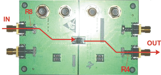
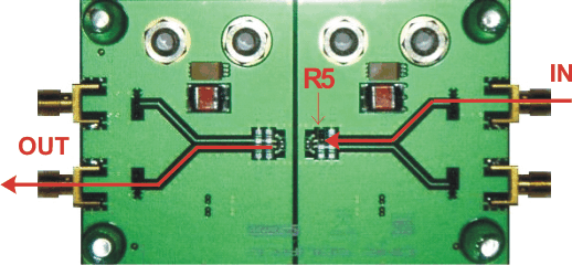
The ISO721EVM configuration has an SMA connector J3 set up as the input to pin 2, the IN pin of the ISO721 in Figure 3-1 and Figure 4-1. A 0-Ω input series resistor, R8, is located next to the J3 input connector, and a 50-Ω R5 from the input to ground is located on the bottom of the board.
 Figure 5-1 ISO721 and ISO721M EVM, Top
The output channel configuration of the ISO721EVM has the OUT pin (pin 6) of Figure 3-1 and Figure 4-1 connected to SMA connector J2 through a 0- Ω series resistor R4.
 Figure 5-2 ISO721 and ISO721M EVM, Bottom
The pads for R3, C12, and C13 are available on the bottom of the EVM for varied loading conditions if desired by a user.