SLLA600 October 2022 THVD8000 , THVD8010
3 Simulating the New System
To show how the simulation file should be set up two different examples are going to be shown to clarify the process as well as show results. A list of assumptions that are used through the simulation process are shown below.
- Assumption 1: The system is very linear under normal operating conditions so superposition is used to remove the power source from the analysis – since it the noise on power nodes is independent of the source. This is valid as during normal operating conditions the THVD80x0 Device Family operates in a very linear manner.
- Assumption 2: The THVD80x0 device is replaced with a differential source of value 1V so it easy to scale up to what the actual output voltage is in the specific system. This assumes the parasitics of the THVD80x0 output circuit doesn’t greatly affect the noise on the power nodes.
- The negative terminal of the source is grounded as Simulations tend to have issues with floating nodes. However, the Output differential voltage remains the same.
- Assumption 4: The AC power source has contact resistance of 50 mΩ on both the positive and negative terminals. This could be smaller or larger so a small resistance was used to model the contact resistance.
- Assumption 5: The THVD80x0 Devices have an input impedance, when in receive mode, of a constant 96 KΩ. This will vary based on input voltage but 96 KΩ is a common stand-in for 1/8 Unit Load Devices Input Impedance.
- Assumption 6: Transmission Line and High Frequency Circuit Considerations are neglected in the simulation as through proper design it should only add a small amount of attenuation to the signal depending on distance.
Example 3.1: 2 Node System; 36VAC @ 60Hz that can provide 4A of current, Power load is requesting 3.6A, Modulation Frequency = 125KHz, 120 Terminations Used.
- Assume capacitor between communication node and shared power/data bus has an impedance at the modulation frequency of 5 Ohms. Using Equation 7 yields C ~ 255nF.
- Since this is a low node count system (2 Nodes) Equation 10 can be used and it yields a minimum inductance value of ~942uH per node.
- Calculate extra current budget by subtracting
requested current from max current possible from source. For this example, that
would be 4 – 3.6 = 400 mA of extra current available for filter caps.
- As a note all 400 mA need to be consumed by the filtering capacitor – but this will provide the lowest impedance possible for the THVD80x0 Device.
- Calculate extra current per load by dividing available current by the number of nodes – so in the example it would be 400 mA / 2 which yields 200 mA per node.
- The minimum impedance that this filter capacitor can be is the source voltage peak divided by the maximum current for the filtering capacitor in each node – so it would be 36 V/200 mA which yields 180 Ω
- Find the capacitance that has an impedance magnitude of 180 Ω at power source frequency – for this example that would be approximately 14.7 4uF.:
Figure 3-1 is the simulation profile to see system impact without the AC filtering caps added.
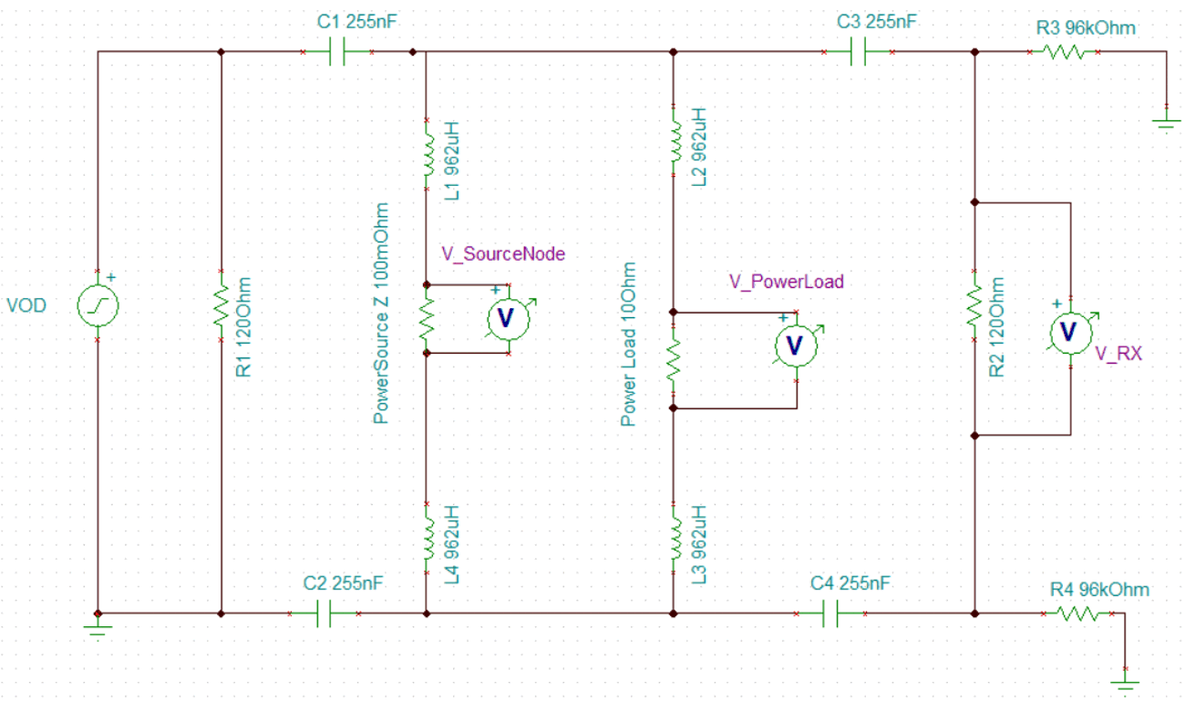 Figure 3-1 Simulation Profile, Without Filtering Capacitors
Without adding the filtering capacitor, the power nodes have more data signal leaking into them.
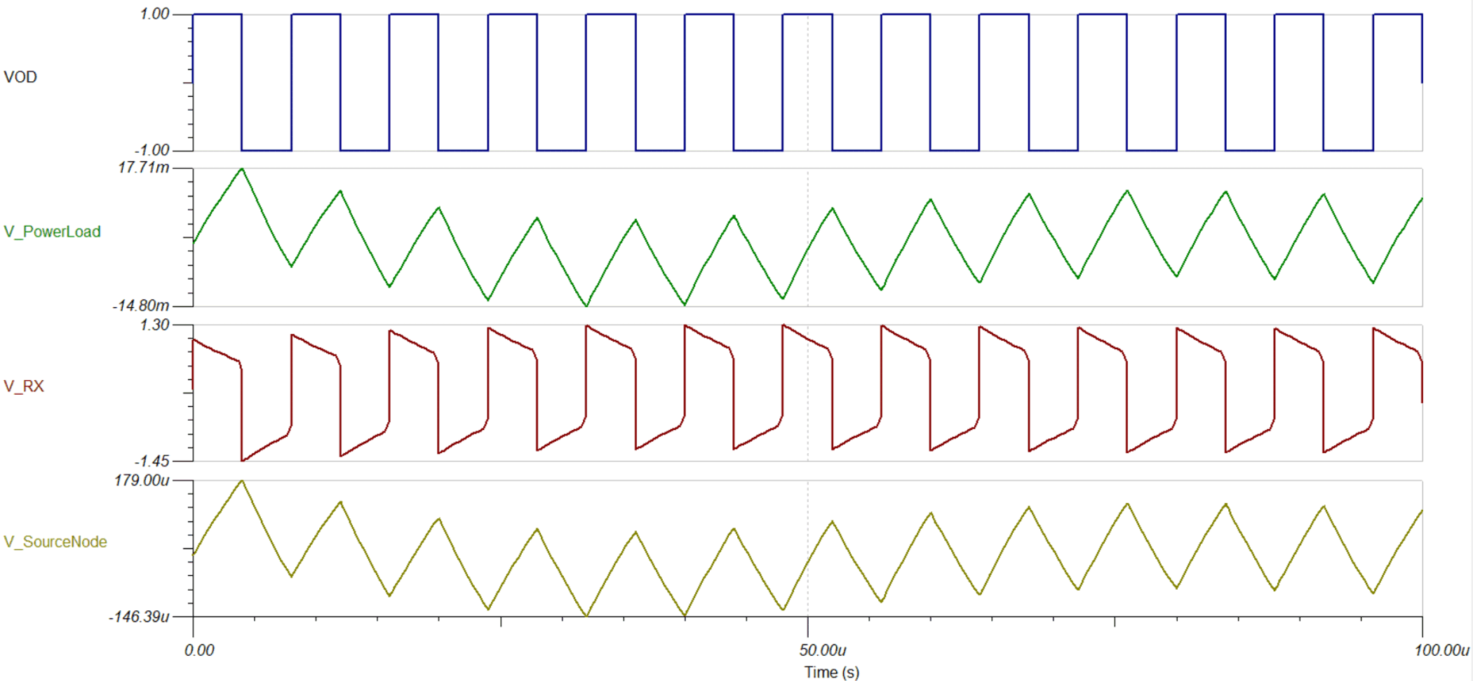 Figure 3-2 Simulation Results, Without Filtering Capacitors
The green signal is the modulated data stream present at the power node. It steadies out at a ripple magnitude of approximately 12 mV – or 1.2% of the data signal is present at the power node. Since the VAC source was shorted for the simulation only the contact impedance remained and shown with the yellow signal, however, since this was very small, the noise on the source node is also small by about a factor of 100 lower than seen on the power load. The received voltage is not being attenuated but has a small gain due to the passive network at 125 KHz.
Figure 3-3 is the simulation profile with the filtering capacitor added.
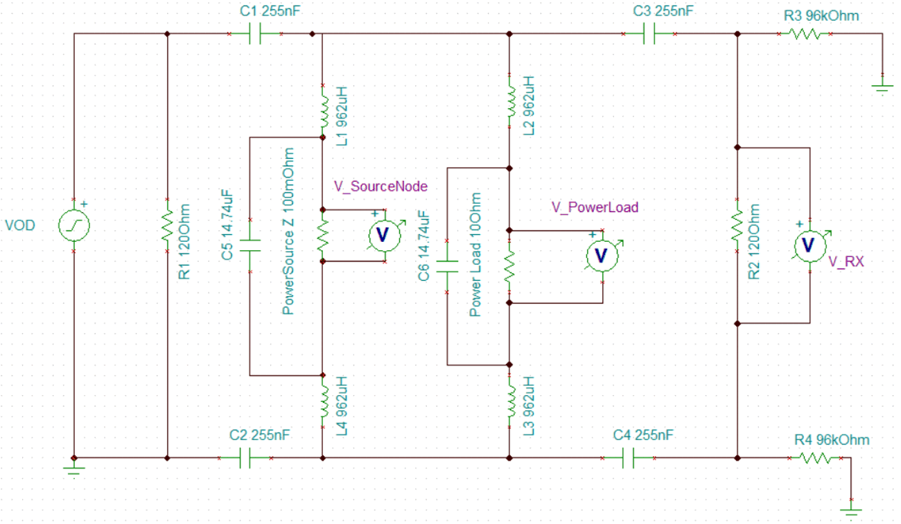 Figure 3-3 Simulation Profile, With Filtering Capacitors
Due to the additional capacitance the settling time has increased so a 500 us simulation was used compared to the 100 us of the first case.
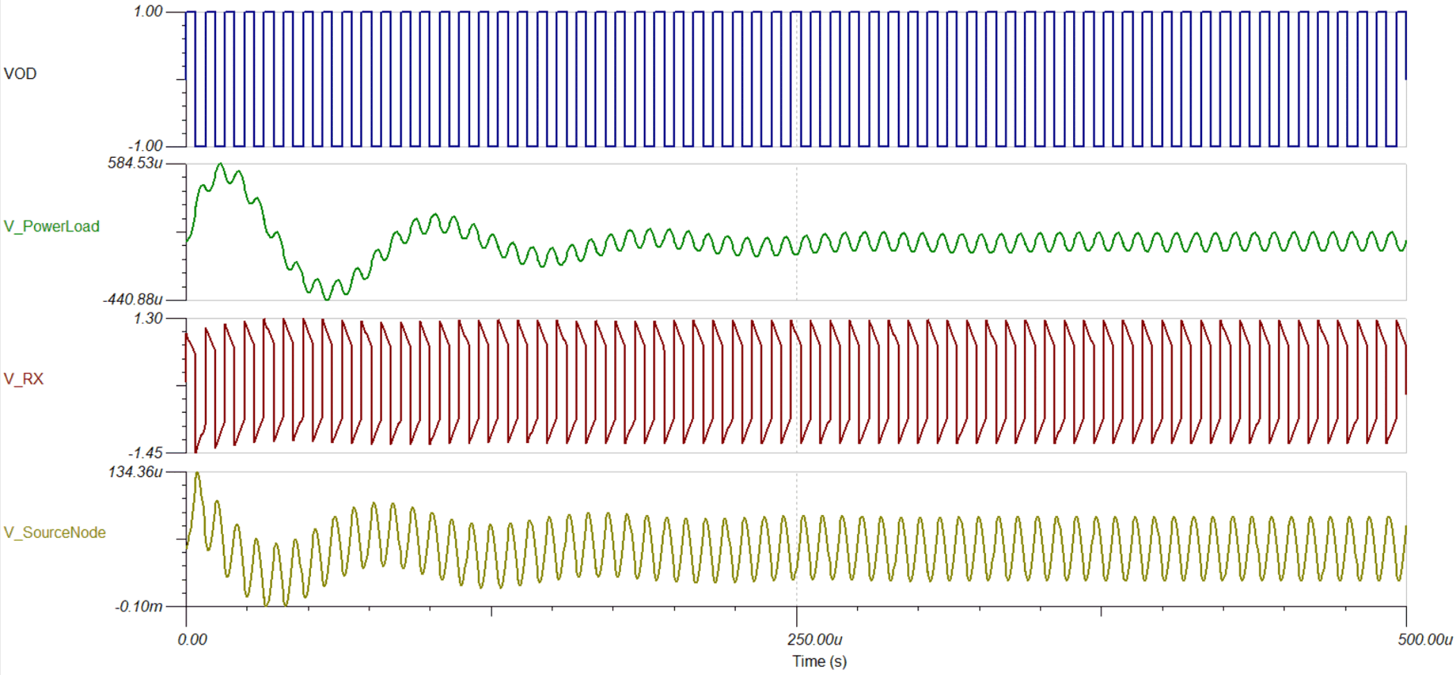 Figure 3-4 Simulation Results, With Filtering Capacitors
The peak signal on the power load is now ~585 uV or 0.0585% of the differential signal. It does take longer to steady out but when it reaches steady state the voltage on this node is about 70 uV or 0.07% of the differential signal. The source node also sees a slight improvement, but this was already small to begin with due to the analysis using superposition to short the AC source.
Example 3.2: 4 Node System; 24VAC at 50 Hz that can provide 5A of current, Power load 1 is requesting 3.6 A, Power load 2 is requesting 0.75 A, and Power load 3 is requesting 0.55 A, Modulation Frequency = 500 KHz, 120 Ohm Terminations Used.
Using the same process as Example 3.1:
- Equation 7 yields a capacitor value of ~64nF.
- To keep error low since this system has > 3 nodes equation 1.8 is used for the inductor value which yields a value of approximately 119 uH.
- There is a total current possible of 5A with 3 sources requesting a total of 4.9 A which leaves 100 mA left over.
- Since there are 5 nodes each node can sink another 20 mA without overstressing the AC source.
- The minimum impedance is the source voltage divided by the extra current per node so 24 V/0.02 A which yields 2.4 KΩ.
- Converting that impedance to a capacitance value yields approximately 1.33 uF
- Setup the simulation as shown in Figure 3-5.
 Figure 3-5 Simulation Profile, Without Filtering Capacitors
If there are difficulties running as a transient simulation try to run as a steady state simulation.
Since only two nodes are terminated the other device are essentially CR filters to ground. The simulation results without the capacitor are shown in Figure 3-6.
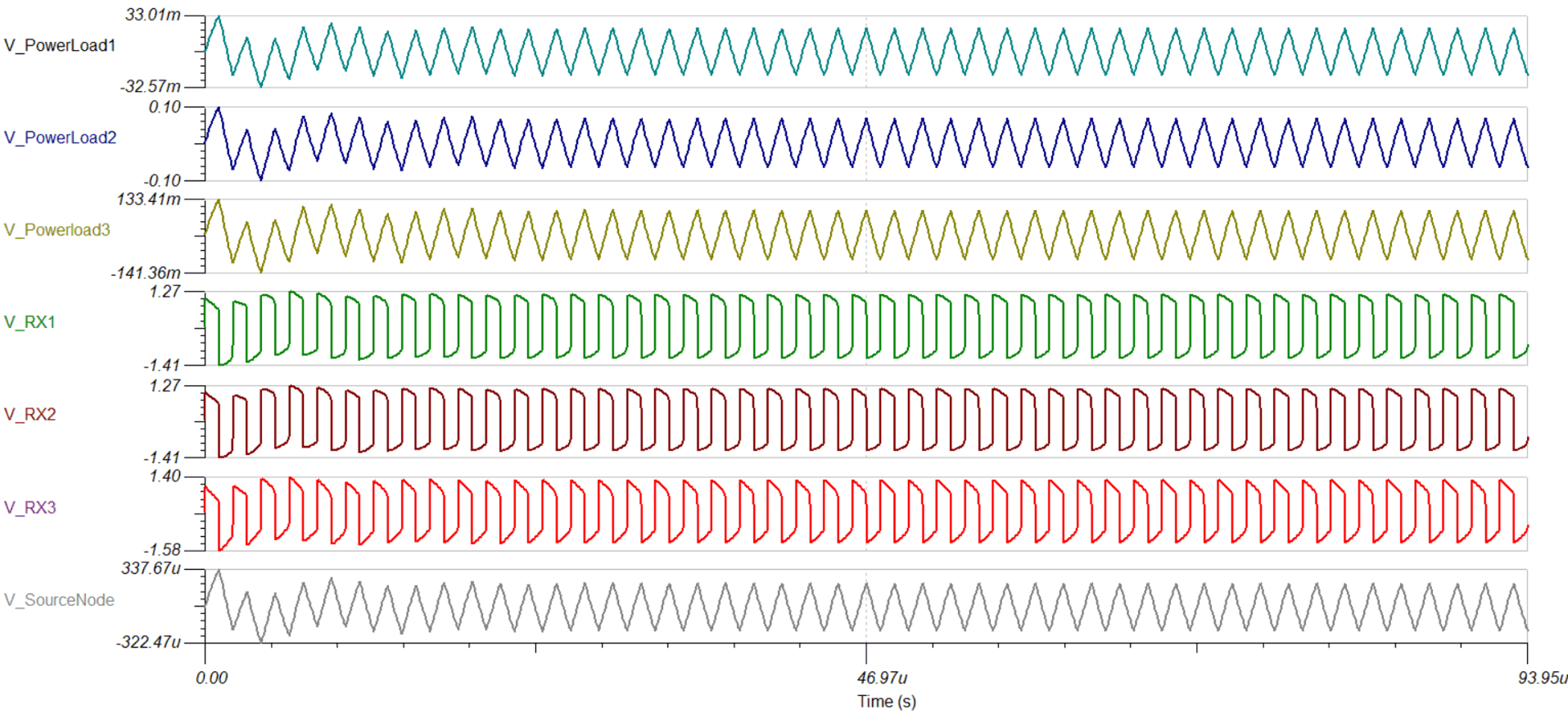 Figure 3-6 Simulation Results, Without Filtering Capacitors
The data stream leaks into the power load nodes depending on how resistive the load is. In this system power node 1 peaks around a magnitude of 3.3% of the differential voltage signal at this node and approaches a steady state magnitude of 1.8% to 2% of the differential voltage signal. Power node 2 peaks at 10% of the data signal and approaches a steady state magnitude of 6.4% to 6.6%. Power node 3 peaks at approximately 13% of the data signal and approaches a steady state magnitude of 8.3% to 9% of the differential voltage signal.
With the baseline approximated – the improvement can also be approximated by adding a 1.33 uF capacitor across each power load and the power source. Which yields the following simulation profile and results.
 Figure 3-7 Simulation Profile, With Filtering Capacitors
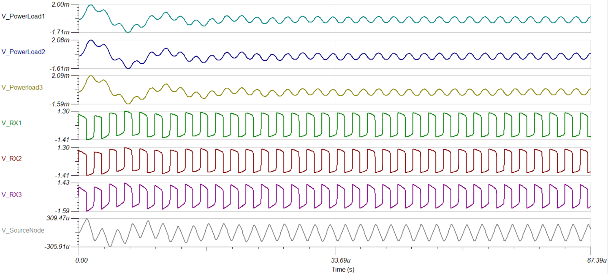 Figure 3-8 Simulation Results, With Filtering Capacitors
Where power load 1 now peaks at ~0.2% of the incoming differential signal and approaches a steady state magnitude of 0.04%. Power load 2 peaks at 0.208% of the incoming signal and approaches a steady state magnitude of 0.04% - the same as power load 1. Finally, power load 3 peaks at 0.209% of the incoming signal and approaches a steady state of ~0.04% the same as the first two loads.