SLLA566A September 2021 – October 2021 SN6501 , SN6501-Q1 , SN6505A , SN6505A-Q1 , SN6505B , SN6505B-Q1 , SN6505D-Q1 , SN6507-Q1
3 Test Results
The test environment for this data was previously developed with careful consideration for parameters and parasitic components that could interfere with accurate emissions results. The design guidelines include following a symmetrical layout pattern as shown in Figure 3-1 and measuring the differences in the circuit’s behavior with and without a snubber circuit.
The transformer selected for these tests is shown with its measured parameters listed in Table 3-1, and its values represent a sample of commercially-available transformers on the market today. The primary inductance, leakage inductance, and parasitic capacitance of the isolation transformer were measured directly on the transformer before it was mounted to the test PCB, and the capacitance of D1/D2 traces was also measured before the transformer was mounted onto the test PCB using an LCR meter with SN6505B powered at 5 V and its EN pin tied LOW.
| Transformer | Primary inductance (1-3) | Leakage inductance (1-3, tie secondary side pins) | Parasitic capacitance (tie 1, 2, 3 and 4, 5, 6) | D1/D2 trace capacitance |
|---|---|---|---|---|
| PH9085.011NL (Pulse) | 1.02mH | 443nH | 13.2pF | 118pF |
Reducing radiated emissions in push-pull isolated power supplies centers around critically damping the resonance frequency caused by the parasitics in the switching path on D1 and D2 pins of the SN6501 and SN6505. For the following snubber circuit calculations, the resonant frequency was measured on an oscilloscope using active probes.
The impedance of the resistor in the snubber circuit should match the impedance of the switching frequency in order to critically damp the resonating energy while the capacitor blocks DC at lower frequencies and helps reduce power consumption. For this article, the snubber circuit was connected on the primary side of the isolated power supply circuit, as shown in Figure 3-1.
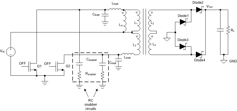 Figure 3-1 Test PCB Configuration with Snubber Circuits
The following procedure was used to determine the appropriate snubber circuit values for circuits using the PH9085.011NL transformer shown in Figure 3-1.
- Measure the resonance frequency, fresonance, of spikes on D1/D2 switching waveforms using an oscilloscope.
- Measure the parasitic capacitance, CPAR, of D1/D2 switching traces using an LCR meter.
- Using the measured fresonance and CPAR, parasitic inductance can be calculated by:Equation 6.
- Characteristic impedance, Zchar, of the resonance can be determined by:Equation 7.
- Rsnubber in the RC snubber circuit should equal Zchar above, and the capacitor, Csnubber, should be sized to be multiple times the parasitic capacitance, CPAR. A factor of about 7x was chosen for the measurements in this document.
The measurements for each of the steps above can be found in Table 3-2, followed by conducted and radiated emissions measurements of the PCB and transformer with and without its respective snubber circuit for comparison in Figure 3-2, Figure 3-3, Figure 3-4, Figure 3-6, and Figure 3-7.
| Transformer | Measured resonance frequency | Measured D1/D2 trace capacitance | Calculated parasitic inductance | Calculated Zchar | Calculated snubber circuit | Actual snubber circuit |
|---|---|---|---|---|---|---|
| PH9085.011NL (Pulse) | 59MHz | 128.5pF | 56.6nH | 20.99Ω | R = 21Ω, C = 899.5pF | R = 22Ω, C = 820pF |
Figure 3-2 and Figure 3-3 are two time-domain waveforms showing the initially measured resonance frequency for the calculation steps above in Figure 3-2 and the resulting dampened time domain waveform once the snubber circuit was included in Figure 3-3:
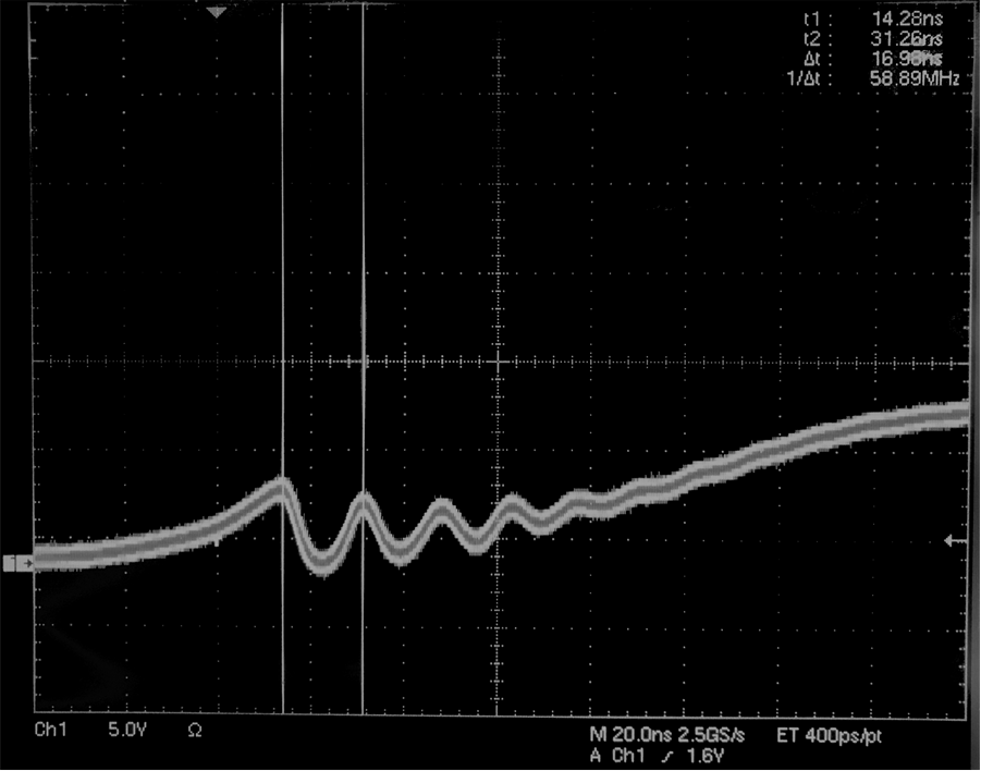 Figure 3-2 PH9085.011NL Time Domain D1/D2 Infinite Persistence Waveform without RC Snubber
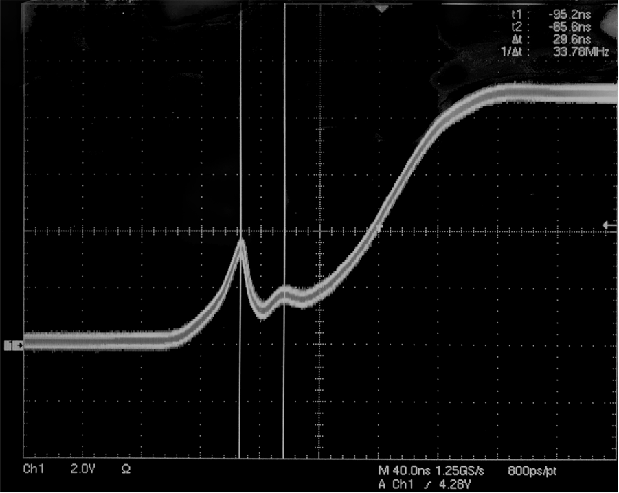 Figure 3-3 PH9085.011NL Time Domain D1/D2 Infinite Persistence Waveform with 22Ω, 820pF Snubber
In Figure 3-4, conducted emissions measurements of the PCB with and without the snubber circuit show a conducted emissions reduction of about 12dB with the snubber at the measured resonance frequency, 59MHz, and a reduction of about 7dB at 100MHz before converging to the noise floor:
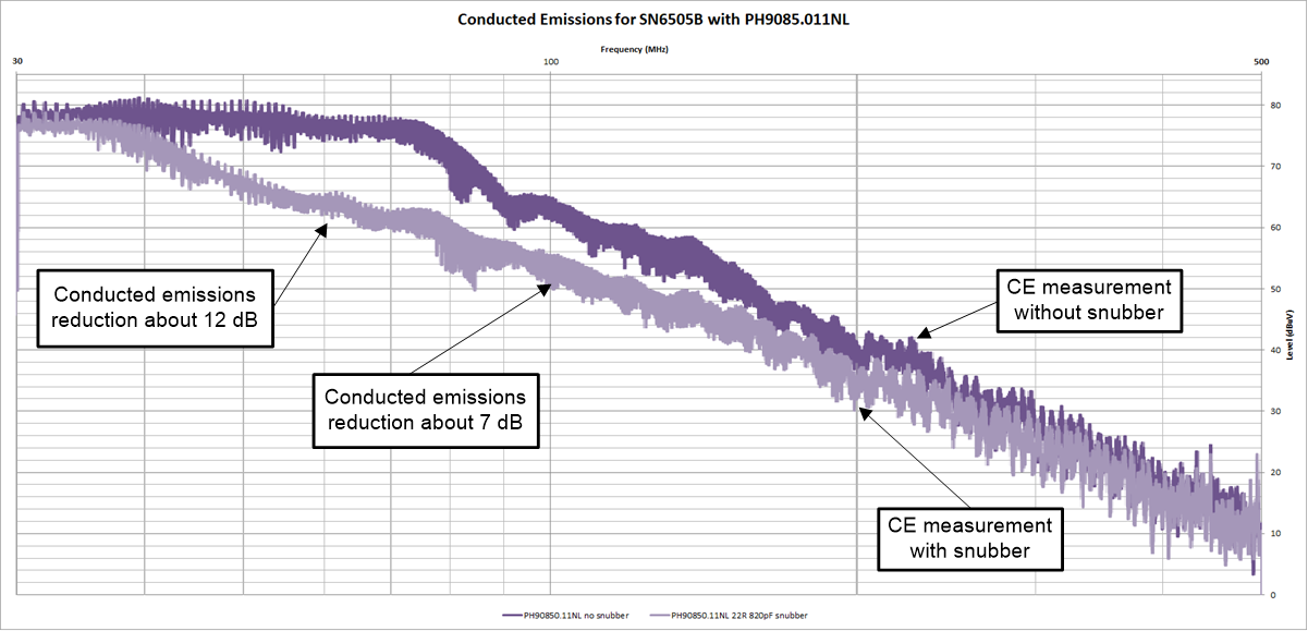 Figure 3-4 Conducted Emissions Comparison With and Without Snubber for this PCB with PH9085.011NL
For radiated emissions measurements, a 1m cable was connected to the isolated GND plane to simulate real-world scenarios where long boards and I/O cables amplify emissions. The radiated emissions test environment is shown in Figure 3-5 with resulting data in Figure 3-6 and Figure 3-7. These results show the snubber was effective in reducing radiated emissions about 5dBμV/m at 59MHz and about 13dBμV/m at 100MHz:
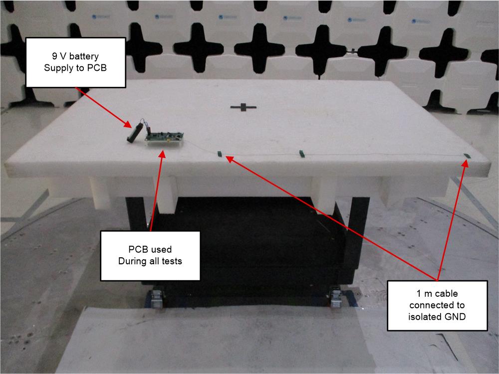 Figure 3-5 Radiated Emissions Test Environment per CISPR32
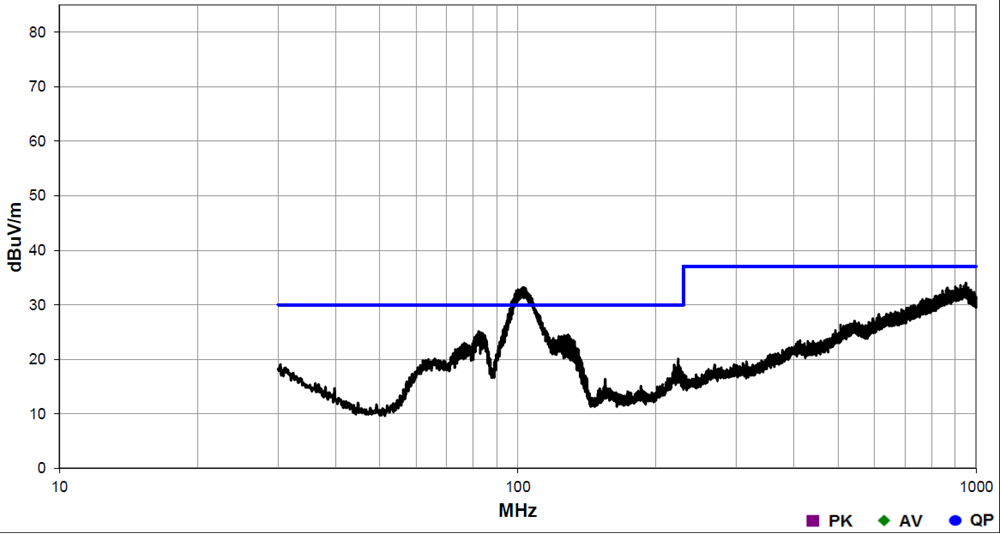 Figure 3-6 Horizontal Radiated Emissions Measurements per CISPR32 Class B for PH9085.011NL with 1m Cable on Isolated GND and no Snubber
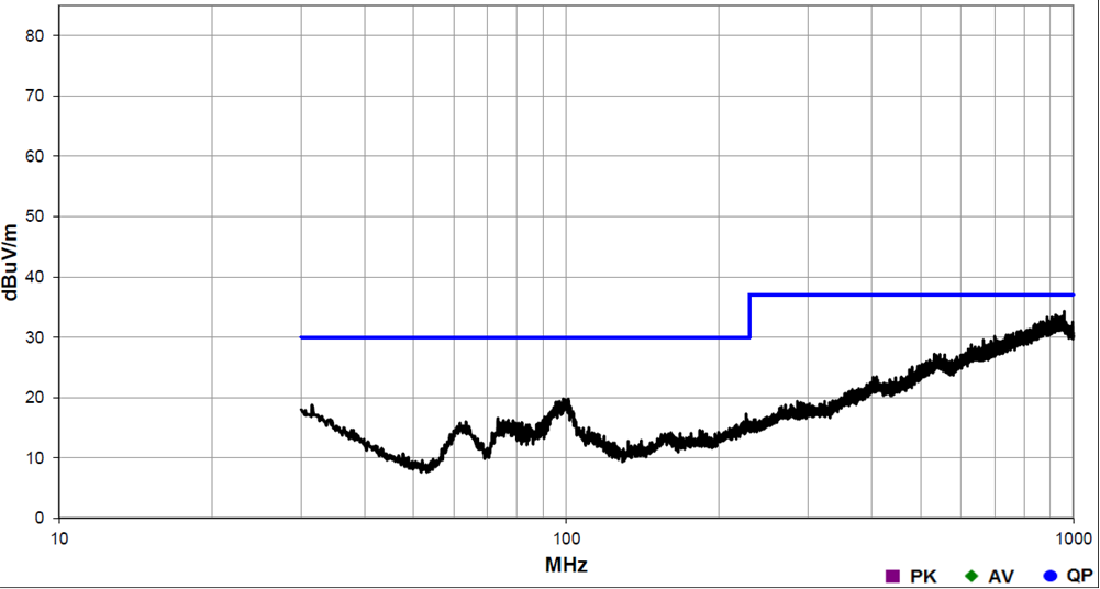 Figure 3-7 Horizontal Radiated Emissions Measurements per CISPR32 Class B for PH9085.011NL with 1m Cable on Isolated GND and 22Ω, 820pF Snubber