SLAT161 June 2022 HD3SS3411 , TMUXHS4412
2.1 PCIe Link
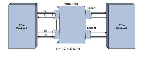
Before considering clocking architectures, examine the PCIe data link. It consists of one or more lanes that provide a transmit (Tx) and receive (Rx) differential pair. Figure 2-1 shows two devices that need to transfer data. One of the key advantages of PCIe is its bandwidth scalability enabling up to 32 lanes to be configured on a single link. Table 2-1 is the data rate vs different PCIe standard.
 Figure 2-1 PCIe Link
Table 2-1 PCIe Standard Versus Bit
Rate
| PCIe Standard | Raw Bit Rate |
|---|---|
| PCIe 1.1 | 2.5 GBit/s |
| PCIe 2.1 | 5.0 GBit/s |
| PCIe 3.1 | 8.0 GBit/s |
| PCIe 4.0 | 16.0 GBit/s |
| PCIe 5.0 | 32.0 GBit/s |