SLAAEB0 December 2023 MSPM0G1105 , MSPM0G1106 , MSPM0G1107 , MSPM0G1505 , MSPM0G1506 , MSPM0G1507 , MSPM0G3105 , MSPM0G3106 , MSPM0G3107 , MSPM0G3107-Q1 , MSPM0G3505 , MSPM0G3506 , MSPM0G3507 , MSPM0G3507-Q1 , MSPM0L1105 , MSPM0L1106 , MSPM0L1303 , MSPM0L1304 , MSPM0L1305 , MSPM0L1306 , MSPM0L1343 , MSPM0L1344 , MSPM0L1345 , MSPM0L1346
Description
The ADC to I2C subsystem example demonstrates how to use the internal ADC to convert an analog signal into a digital representation and transfer the result through I2C. The example configures the MCU to act as an external ADC, receive I2C commands from an I2C controller, and execute the received command accordingly. With simple example commands provided, users can utilize the framework to implement their own commands. Optionally, the MCU can also process the ADC data before transmitting the data via I2C, which is especially useful in applications that need to process the raw data into meaningful values. Download the code for the ADC to I2C Subsystem here.
The following figure shows a block diagram of the system.
 Figure 1-1 Subsystem Functional Block Diagram
Required Peripherals
The application requires the internal ADC and 1 instance of the I2C.
| Sub-block Functionality | Peripheral Used | Notes |
|---|---|---|
| Analog signal capture | ADC | Called ADC12_0_INST in code |
| Sending ADC data | I2C | Device is the target for this example |
Compatible Devices
Based on the requirements in the Required Peripherals table some compatible devices and corresponding EVMs are listed below. Other MSPM0 devices can be used with this subsystem as long as they have the required peripherals.
| Compatible Devices | EVM |
|---|---|
| MSPM0Lxxx | LP-MSPM0L1306 |
| MSPM0Gxxx | LP-MSPM0G3507 |
Design Steps
- Determine the configuration for the ADC including reference source, reference value, and sampling rate based on the expected analog input and design requirements.
- Configure the ADC in SysConfig based on requirements in the previous step.
- Configure the I2C peripheral in SysConfig, setting the I2C in target mode.
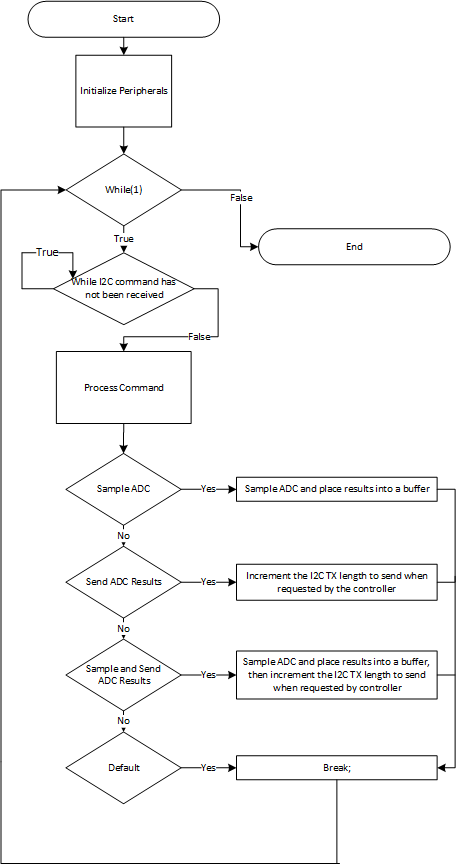
- Write Application Code to transfer the ADC data from the memory registers to the I2C TX FIFO. See the Software Flowchart for an overview or view the code directly.
Design Considerations
- Max Sampling Speed: The sampling speed of the ADC is based on input signal frequency, analog front end, filters or any other design parameters that affect sampling.
- ADC Reference: Choose the reference to align with the expected max input to utilize the full scale range of the ADC.
- Clock Settings: The clock source determined the total time for sample and conversion time. The clock divider in tandem with the SCOMP setting determines the total sampling time. SysConfig sets the appropriate SCOMP depending on the sampling time setting.
- I2C configurations can be adjusted depending on your controller needs, such as the I2C address, addressing mode, glitch filters, clock stretching, and more.
Software Flow Chart