SLAAE46 November 2021 DAC43701
3.3 DAC Pseudo Code Example
This section gives a pseudo code example for the design goals in Table 3-1. From Equation 1, the DAC_DATA register should be 14h and D9h for VDAC- and VDAC+ respectively. To generate the customized square wave, MCU can update the DAC_DATA at a frequency of 140Hz through I2C.
Pseudo Code Example for Programmable Square Wave VCOM
//SYNTAX:WRITE <REGISTER NAME (REGISTER ADDRESS)>, <MSB DATA>, <LSB DATA>
//Enable output, use VDD as DAC reference,
WRITE GENERAL_CONFIG (0xD1), 0x01, 0xE0
WHILE ()
{
//Write DAC code (12-bit aligned), For 2.6-V VDD as DAC reference, the 8-bit hex code for 0.2 V is 0x14
//Left aligned this becomes 0x0140
WRITE DAC_DATA(0x21), 0x01, 0x40
//Duration is 1/280 second
DELAY(1/280)
//Write DAC code (12-bit aligned), For 2.6-V VDD as DAC reference, the 8-bit hex code for 2.2 V is 0xD9
//Left aligned this becomes 0x0D90
WRITE DAC_DATA(0x21), 0x0D, 0x90
//Duration is 1/280 second
DELAY(1/280)
}
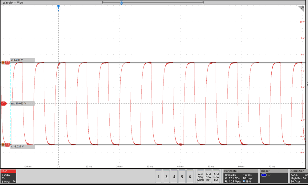
Figure 3-3 shows the test results
 Figure 3-3 VCOM Test Result