SLAA946 April 2021 AFE10004
3 Sequencing
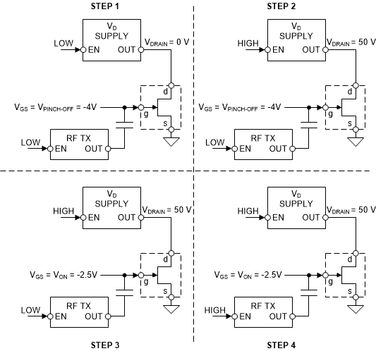
Powering the FET on and off in a controlled routine is necessary to prevent the VGS voltage from being too high when the VD is applied. Such a state causes the FET to operate in saturation mode, and thermal damage the FET or board that it is mounted on. Powering on a FET requires the following steps:
- The first signal to be applied to the FET must be VGS. The VGS voltage must transition to the VGS pinch-off voltage or lower. This ensures that when the VD voltage is applied, the gate is already low.
- Next, the drain voltage supply can be enabled, allowing the VD to be powered to the nominal value (50 V, for example). Remember that as the VGS is at the pinch-off voltage, IDS must be minimal.
- Now that the VD is applied, the VGS bias voltage can be increased to set the desired power output of the PA.
- Finally, the RF signal can be enabled. This allows the FET to transmit a signal.
 Figure 3-1 GaN Power Sequencing
The PA can be safely shut down by reversing the power-on steps.
- Disable the RF signal from the FET.
- Reduce the VGS voltage to the pinch-off value, eliminating the power output of the FET.
- Disable the VD voltage by sending a disable signal to the drain supply.
- Finally, the VGS voltage can be allowed to collapse to ground as the PA is fully disabled.