SFFSBF8 June 2026 LM654B0-Q1
4 Pin Failure Mode Analysis (Pin FMA)
This section provides a failure mode analysis (FMA) for the pins of the LM654B0-Q1, LM654A5-Q1, LM654A2-Q1, and LM654A0-Q1. The failure modes covered in this document include the typical pin-by-pin failure scenarios:
- Pin short-circuited to ground (see Table 4-2)
- Pin open-circuited (see Table 4-3)
- Pin short-circuited to adjacent pin (see Table 4-4)
- Pin short-circuited to supply (see Table 4-5)
Table 4-2 through Table 4-5 also indicate how these pin conditions can affect the device as per the failure effects classification in Table 4-1.
| Class | Failure Effects |
|---|---|
| A | Potential device damage that affects functionality. |
| B | No device damage, but loss of functionality. |
| C | No device damage, but performance degradation. |
| D | No device damage, no impact to functionality or performance. |
Below is the LM654B0-Q1, LM654A5-Q1, LM654A2-Q1, and LM654A0-Q1 pin diagram package. For a detailed description of the device pins, see the Pin Configuration and Functions section in the LM654B0-Q1, LM654A5-Q1, LM654A2-Q1, and LM654A0-Q1 datasheets.
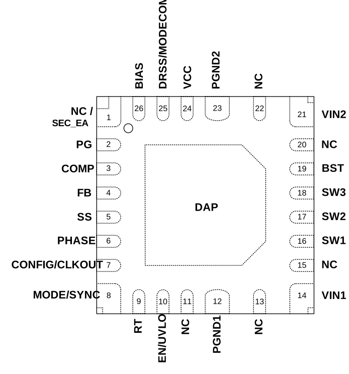 Figure 4-1 LM654B0-Q1, LM654A5-Q1,
LM654A2-Q1, and LM654A0-Q1 Pin Diagram
Figure 4-1 LM654B0-Q1, LM654A5-Q1,
LM654A2-Q1, and LM654A0-Q1 Pin Diagram | Pin Name | Pin No | Description of Potential Failure Effects | Failure Effect Class |
|---|---|---|---|
| NC / SEC_EA | 1 | When CNFG is set to primary, the device operates as normal. | D |
| When CNFG is set to secondary, the device gain is reduced, increasing deviation during transients. | C | ||
| NC | 11 | The device operates as normal. | D |
| 13 | |||
| 15 | |||
| 20 | |||
| 22 | |||
| PG | 2 | There is a loss of Power Good functionality. | B |
| COMP | 3 | When there is internal compensation, the device operates as normal. | D |
| When there is external compensation, there is a loss of regulation. VOUT = 0V. | B | ||
| FB | 4 | When VOUT is fixed at 3.3V, the FB pin is shorted to ground by default. The device operates as normal. | D |
| When VOUT is fixed at 5V, the VCC pin shorts to ground. There is a loss of regulation. VOUT = 0V. | B | ||
| When VOUT is adjustable, there is a loss of regulation. VOUT = VIN. | B | ||
| SS | 5 | There is a loss of regulation. VOUT = 0V. | B |
| PHASE | 6 | The device loses phase information and there can be an increased output voltage ripple. | C |
| CNFG/SYNCOUT | 7 | There is a loss of regulation. VOUT = 0V. | B |
| MODE/SYNC | 8 | In AUTO mode, the device operates as normal. | D |
| In FPWM mode, there is a loss of regulation. VOUT = 0V. | B | ||
| In external SYNC, there is a loss of synchronization. The performance of the device degrades. The device operates in AUTO mode. | C | ||
| RT | 9 | When the frequency is fixed at 400kHz, there is a loss of regulation. VOUT = 0V. | B |
| When the frequency is fixed at 2.2MHz, the device operates as normal. | D | ||
| When the frequency is adjustable, the performance of the device degrades. The device switches at 2.2MHz. | C | ||
| EN/UVLO | 10 | The device disables. VOUT = 0V. | D |
| PGND1, PGND2 | 12 | The device operates as normal. | D |
| 23 | |||
| VIN1, VIN2 | 14 | VOUT = 0V. | B |
| 21 | |||
| SW1, SW2, SW3 | 16 | The device is damaged. | A |
| 17 | |||
| 18 | |||
| BST | 19 | There is a loss of regulation. VOUT = 0V. | B |
| VCC | 24 | There is a loss of regulation. VOUT = 0V. | B |
| DRSS/MCOMM | 25 | The DRSS pin is disabled. Slew rate control is disabled. The performance of EMI degrades. | C |
| BIAS | 26 | When the BIAS pin is tied to VOUT, there is a loss of regulation. VOUT = 0V. | B |
| When the BIAS pin is tied to ground, the device operates as normal. | D |
| Pin Name | Pin No | Description of Potential Failure Effects | Failure Effect Class |
|---|---|---|---|
| NC / SEC_EA | 1 | When CNFG is set to primary, the device operates as normal. | D |
| When CNFG is set to secondary, the secondary can be operated in open loop, depending on the FB configuration and lose regulation. | B | ||
| NC | 11 | The device operates as normal. | D |
| 13 | |||
| 15 | |||
| 20 | |||
| 22 | |||
| PG | 2 | There is a loss of Power Good functionality. | B |
| COMP | 3 | When there is internal compensation, the device operates as normal. | D |
| When there is external compensation, the performance of the device degrades. | C | ||
| FB | 4 | When VOUT is fixed, there is a loss of regulation. VOUT = 0V. | B |
| When VOUT is adjustable, there is a loss of regulation. VOUT = VIN. | B | ||
| SS | 5 | The device operates as normal. | D |
| PHASE | 6 | The device loses phase information and there can be an increased output voltage ripple. | C |
| CNFG/SYNCOUT | 7 | There is a loss of regulation. VOUT = 0V. | B |
| MODE/SYNC | 8 | In AUTO mode, the device operates as normal. | D |
| In FPWM mode, the AUTO operation occurs in the next cycle. The performance of the device degrades. | C | ||
| In external SYNC, there is a loss of synchronization. The device operates in AUTO mode. The performance of the device degrades. | C | ||
| RT | 9 | When the frequency is fixed at 400kHz, the performance of the device degrades. The device operates at 2.2MHz. | C |
| When the frequency is fixed at 2.2MHz, the device operates as normal. | D | ||
| When the frequency is adjustable, the performance of the device degrades. The device operates at 2.2MHz. | C | ||
| EN/UVLO | 10 | The device disables. VOUT = 0V. | B |
| PGND1, PGND2 | 12 | The degradation in performance depends on the conditions of the application. | C |
| 23 | |||
| VIN1, VIN2 | 14 | The degradation in performance depends on the conditions of the application. | C |
| 21 | |||
| SW1, SW2, SW3 | 16 | The degradation in performance depends on the conditions of the application. | C |
| 17 | |||
| 18 | |||
| BST | 19 | There is a loss of regulation. VOUT = 0V. | B |
| VCC | 24 | The LDO operation is unstable. There is a loss of regulation. | B |
| DRSS/MCOMM | 25 | The DRSS pin is enabled. The slew rate control is enabled. The device operates as normal. | D |
| BIAS | 26 | When VOUT is fixed, there is a loss of regulation. VOUT = 0V. | B |
| When VOUT is adjustable, the performance of the device degrades. The IQ is higher. | C |
| Pin Name | Adjacent Pin | Description of Potential Failure Effects | Failure Effect Class |
|---|---|---|---|
| NC / SEC_EA | PG | When CNFG is set to primary, the device operates as normal. | D |
| When CNFG is set to secondary, SEC_EA is grounded. There is a loss of Power Good functionality. | B | ||
| When CNFG is set to secondary, SEC_EA is tied to VCC. The device is damaged if PG > 20V. Use resistor pullup to limit current to VCC to prevent damage. | A | ||
| PG | COMP | When there is internal compensation, there is a loss of Power Good functionality. | B |
| When there is external compensation, there is a loss of regulation. | B | ||
| COMP | FB | When there is external compensation, and VOUT is fixed at 3.3V, there is a loss of regulation. VOUT = 0. | B |
| When there is external compensation, and VOUT is fixed at 5V, there is a loss of regulation. There is an overvoltage condition. | B | ||
| When there is external compensation, and VOUT is adjustable, there is a loss of regulation. There is an overvoltage condition. | B | ||
| FB | SS | When VOUT is fixed at 3.3V, there is a loss of regulation. VOUT = 0. | B |
| When VOUT is fixed at 5V, there is a loss of regulation. VOUT = 0. | B | ||
| When VOUT is adjustable, there is a loss of regulation. | B | ||
| SS | PHASE | There can be a loss of regulation when PHASE < 1V setting. VOUT = 0V. | B |
| PHASE | CNFG/SYNCOUT | PHASE is tied to ground. There is a loss of regulation. | B |
| PHASE is tied to VCC. There is a loss of external compensation. | B | ||
| When CNFG is set to secondary. The device loses phase information and there can be an increased output voltage ripple. | C | ||
| CNFG/SYNCOUT | MODE/SYNC | When there is internal compensation (COMP pin tied to VCC), the device operates in FPWM mode. | D |
| When there is external compensation (COMP pin pulled to GND with a 49.9kΩ resistor), the device operates in AUTO mode. | D | ||
| MODE/SYNC | RT | The RT pin is tied to GND and the MODE pin is tied to GND. The device operates as normal. | D |
| The RT pin is tied to GND and the MODE pin is tied to VCC. There is a loss of regulation. VOUT = 0. | B | ||
| The RT pin is tied to VCC and the MODE pin is tied to GND. There is a loss of regulation. VOUT = 0. | B | ||
| The RT pin is tied to VCC and the MODE pin is tied to VCC. The device operates as normal. | D | ||
| The RT pin is pulled to GND with a resistor and the MODE pin is tied to GND. There is a loss of regulation. | B | ||
| The RT pin is pulled to GND with a resistor and the MODE pin is tied to VCC. There is a loss of regulation. | B | ||
| RT | EN/UVLO | The RT pin is tied to GND and the EN pin is tied to VIN. There is a loss of regulation. VOUT = 0. | B |
| The RT pin is tied to VCC and the EN pin is tied to VIN. The device is damaged. | A | ||
| The RT pin is pulled to GND with a resistor and the EN pin is tied to VIN. The performance of the device degrades. | C | ||
| EN/UVLO | NC | The device operates as normal. | D |
| NC | PGND1 | The device operates as normal. | D |
| PGND1 | NC | The device operates as normal. | D |
| NC | VIN1 | The device operates as normal. | D |
| VIN1 | NC | The device operates as normal. | D |
| NC | SW1 | The device operates as normal. | D |
| SW1 | SW2 | The device operates as normal. | D |
| SW2 | SW3 | The device operates as normal. | D |
| SW3 | BST | There is a loss of regulation. Device damage can occur depending on the timing of the short. | A |
| BST | NC | The device operates as normal. | D |
| NC | VIN2 | The device operates as normal. | D |
| VIN2 | NC | The device operates as normal. | D |
| NC | PGND2 | The device operates as normal. | D |
| PGND2 | VCC | There is a loss of regulation. VOUT = 0V. | B |
| VCC | DRSS/MCOMM | The DRSS pin is tied to VCC. The device operates as normal. | D |
| The DRSS pin is tied to GND. There is a loss of regulation. VOUT = 0V. | B | ||
| The DRSS pin is pulled to GND with a resistor. The performance of the device degrades. | C | ||
| DRSS/MCOMM | BIAS | The DRSS pin is tied to GND and the BIAS pin is tied to GND. The device operates as normal. | D |
| The DRSS pin is tied to VCC and the BIAS pin is tied to GND. There is a loss of regulation. VOUT = 0V. | B | ||
| The DRSS pin is pulled to GND with a resistor and the BIAS pin is tied to GND. The performance of the device degrades. | C | ||
| The DRSS pin is tied to GND and the BIAS pin is tied to VOUT. There is a loss of regulation. | B | ||
| The DRSS pin is tied to VCC and the BIAS pin is tied to VOUT (<5V). The device operates as normal. | D | ||
| The DRSS pin is tied to VCC and the BIAS pin is tied to VOUT (>5V). The device is damaged. | A | ||
| The DRSS pin is pulled to GND with a resistor and the BIAS pin is tied to VOUT. The performance of the device degrades. | C | ||
| BIAS | NC | The device operates as normal. | D |
| Pin Name | Pin No | Description of Potential Failure Effects | Failure Effect Class |
|---|---|---|---|
| NC / SEC_EA | 1 | The device is damaged if supply > 20V. | A |
| NC | 11 | The device operates as normal. | D |
| 13 | |||
| 15 | |||
| 20 | |||
| 22 | |||
| PG | 2 | The device is damaged if supply > Absolute Maximum Rating. | A |
| COMP | 3 | The device is damaged if supply > 5.5V. | A |
| FB | 4 | The device is damaged if supply > 5.5V. | A |
| SS | 5 | The device is damaged if supply > 5.5V. | A |
| PHASE | 6 | The device is damaged if supply > 5.5V. | A |
| CNFG/SYNCOUT | 7 | The device is damaged if supply > 5.5V. | A |
| MODE/SYNC | 8 | The device is damaged if supply > 5.5V. | A |
| RT | 9 | The switching frequency is undefined. The performance of the device degrades. | C |
| EN/UVLO | 10 | The device operates as normal. | D |
| PGND1, PGND2 | 12 | VOUT = 0V. | B |
| 23 | |||
| VIN1, VIN2 | 14 | The device operates as normal. | D |
| 21 | |||
| SW1, SW2, SW3 | 16 | The device is damaged. | A |
| 17 | |||
| 18 | |||
| BST | 19 | The device is damaged. | A |
| VCC | 24 | The device is damaged if supply > 5.5V. | A |
| DRSS/MCOMM | 25 | The device is damaged if supply > Absolute Maximum Rating. | A |
| BIAS | 26 | The device is damaged if supply > Absolute Maximum Rating. | A |