SFFS785 January 2024 TXU0304-Q1
4.1 TSSOP-14 and VQFN-14 Packages
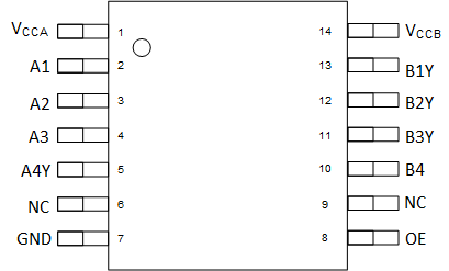
Figure 4-1 shows the TXU0304-Q1 pin diagram for the TSSOP-14 package. For a detailed description of the device pins please refer to the Pin Configuration and Functions section in the TXU0304-Q1 data sheet.
 Figure 4-1 Pin Diagram (TSSOP-14) Package
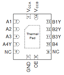
Figure 4-2 shows the TXU0304-Q1 pin diagram for the VQFN-14 package. For a detailed description of the device pins, refer to the Pin Configuration and Functions section in the TXU0304-Q1 data sheet.
 Figure 4-2 Pin Diagram (VQFN-14 Package)
Table 4-2 Pin FMA for Device Pins
Short-Circuited to Ground
| Pin Name | Pin No. | Description of Potential Failure Effect(s) | Failure Effect Class |
|---|---|---|---|
| VCCA | 1 | Device will not be powered or damaged, because short is external to device. System level damage may occur in this scenario. | B |
| A1 | 2 | Ax will be LOW, if corresponding Bx is HIGH, there will be potential damage to the device if the current is not limited. If corresponding Bx is LOW, then nothing will occur, no damage. | B |
| A2 | 3 | B | |
| A3 | 4 | B | |
| A4Y | 5 | B | |
| NC | 6 | Normal operation. | D |
| GND | 7 | Normal operation. | D |
| OE | 8 | All I/Os will be fixed into high impedance (tri-state). | B |
| NC | 9 | Normal operation. | D |
| B4 | 10 | Bx will be LOW, if corresponding Ax is HIGH, there will be potential damage to the device if the current is not limited. If corresponding Ax is LOW, then nothing will occur, no damage. | B |
| B3Y | 11 | B | |
| B2Y | 12 | B | |
| B1Y | 13 | B | |
| VCCB | 14 | Device will not be powered or damaged, because short is external to device. System level damage may occur in this scenario. | B |
Table 4-3 Pin FMA for Device Pins
Open-Circuited
| Pin Name | Pin No. | Description of Potential Failure Effect(s) | Failure Effect Class |
|---|---|---|---|
| VCCA | 1 | Device will not be powered. | B |
| A1 | 2 | Ax input pins will be grounded internally. Ax output pin will in HiZ if device is disabled. If device is enabled, it will be HIGH or LOW depending on the input. | D |
| A2 | 3 | D | |
| A3 | 4 | D | |
| A4Y | 5 | D | |
| NC | 6 | Normal operation. | D |
| GND | 7 | Device will not be powered. | B |
| OE | 8 | I/Os may be High Impedance or active, unknown input state. | A |
| NC | 9 | Normal operation. | D |
| B4Y | 10 | Bx input pin will be grounded internally. Bx output pins will in HiZ if device is disabled. If device is enabled, it will be HIGH or LOW depending on the input. | D |
| B3Y | 11 | D | |
| B2Y | 12 | D | |
| B1Y | 13 | D | |
| VCCB | 14 | Device will not be powered. | B |
Table 4-4 Pin FMA for Device Pins
Short-Circuited to Adjacent Pin
| Pin Name | Pin No. | Shorted to | Description of Potential Failure Effect(s) | Failure Effect Class |
|---|---|---|---|---|
| VCCA | 1 | A1 | Ax will be HIGH, if corresponding Bx is LOW, there will be potential damage to the device if the current is not limited. If corresponding Bx is HIGH, then nothing will occur, no damage. | B |
| A1 | 2 | A2 | Two inputs shorted together will not cause damage unless there is external bus contention that drives the input such that VIL < Input Voltage < VIH in which case excessive supply current to GND may cause damage. One output on VCCA supply is shorted to one input of VCCA supply. Based on the external bus driving this connection, potential high current can be expected if the VILA < Input Voltage A3 < VIHA or if A4Y output gets an undeterministic voltage forced on it in presence of a valid input. | B |
| A2 | 3 | A3 | B | |
| A3 | 4 | A4Y | B | |
| A4Y | 5 | NC | Normal operation. | D |
| NC | 6 | GND | Normal operation. | D |
| GND | 7 | OE | All I/Os will be fixed into high impedance (tri-state). | B |
| OE | 8 | NC | Normal operation. | D |
| NC | 9 | B4 | Normal operation. | D |
| B4 | 10 | B3Y | Two outputs shorted together may cause damage if there is external bus contention that drives one output low while driving the other output high. If both outputs are high or both outputs are low, then nothing will occur, no damage. One output on VCCB supply is shorted to one input of VCCB supply. Based on the external bus driving this connection, potential high current can be expected if the VILB < Input Voltage B4 < VIHA or if B3Y output gets an undeterministic voltage forced on it in presence of a valid input. | A |
| B3Y | 11 | B2Y | A | |
| B2Y | 12 | B1Y | A | |
| B1Y | 13 | VCCB | Bx will be HIGH, if corresponding Ax is LOW, there will be potential damage to the device if the current is not limited. If corresponding Ax is HIGH, then nothing will occur, no damage. | B |
| VCCB | 14 | VCCA | Device will not be powered or damaged, because short is external to device System level damage may occur in this scenario. | B |
Table 4-5 Pin FMA for Device Pins
Short-Circuited to supply
VCCA
| Pin Name | Pin No. | Description of Potential Failure Effect(s) | Failure Effect Class |
|---|---|---|---|
| VCCA | 1 | Normal operation. | D |
| A1 | 2 | Ax will be HIGH, if corresponding Bx is LOW, there will be potential damage to the device if the current is not limited. If corresponding Bx is HIGH, then nothing will occur, no damage. | B |
| A2 | 3 | B | |
| A3 | 4 | B | |
| A4Y | 5 | B | |
| NC | 6 | Normal operation. | D |
| GND | 7 | Device will not be powered or damaged, because short is external to device. System level damage may occur in this scenario. | B |
| OE | 8 | All I/Os will be active, device cannot be disabled. | B |
| NC | 9 | Normal operation. | D |
| B4 | 10 | Bx will be HIGH, if corresponding Ax is LOW, there will be potential damage to the device if the current is not limited. If corresponding Ax is HIGH, then nothing will occur, no damage. | B |
| B3Y | 11 | B | |
| B2Y | 12 | B | |
| B1Y | 13 | B | |
| VCCB | 14 | Device will not be powered or damaged, because short is external to device. System level damage may occur in this scenario. | B |
Table 4-6 Pin FMA for Device Pins
Short-Circuited to supply
VCCB
| Pin Name | Pin No. | Description of Potential Failure Effect(s) | Failure Effect Class |
|---|---|---|---|
| VCCA | 1 | Device will not be powered or damaged, because short is external to device. System level damage may occur in this scenario. | B |
| A1 | 2 | Ax will be HIGH, if corresponding Bx is LOW, there will be potential damage to the device if the current is not limited. If corresponding Bx is HIGH, then nothing will occur, no damage. | B |
| A2 | 3 | B | |
| A3 | 4 | B | |
| A4Y | 5 | B | |
| NC | 6 | Normal operation. | D |
| GND | 7 | Device will not be powered or damaged, because short is external to device. System level damage may occur in this scenario. | B |
| OE | 8 | All I/Os will be active, device cannot be disabled. | B |
| NC | 9 | Normal operation. | D |
| B4 | 10 | Bx will be HIGH, if corresponding Ax is LOW, there will be potential damage to the device if the current is not limited. If corresponding Ax is HIGH, then nothing will occur, no damage. | B |
| B3Y | 11 | B | |
| B2Y | 12 | B | |
| B1Y | 13 | B | |
| VCCB | 14 | Normal operation. | D |