SFFS293 September 2021 TPSM82821 , TPSM82821A , TPSM82822 , TPSM82822A , TPSM82823 , TPSM82823A
2 Pin Failure Mode Analysis (Pin FMA)
This section provides a failure mode analysis (FMA) for the pins of the TPSM8282x. The failure modes covered in this document include the typical pin-by-pin failure scenarios:
- Pin short-circuited to ground (see Table 2-2)
- Pin open-circuited (see Table 2-3)
- Pin short-circuited to an adjacent pin (see Table 2-4)
- Pin short-circuited to VIN (see Table 2-5)
Table 2-2 through Table 2-5 also indicate how these pin conditions can affect the device as per the failure effects classification in Table 2-1.
| Class | Failure Effects |
|---|---|
| A | Potential device damage that affects functionality. |
| B | No device damage, but loss of functionality. |
| C | No device damage, but performance degradation. |
| D | No device damage, no impact to functionality or performance. |
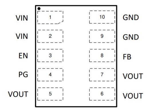
Figure 2-1 shows the TPSM8282x pin diagram. For a detailed description of the device pins, see the Pin Configuration and Functions section in the TPSM8282x data sheet.
 Figure 2-1 Pin Diagram
Following are the assumptions of use and the device configuration assumed for the pin FMA in this section:
- The device is operating in the typical application, please refer to the Simplified Application on the first page in the TPSM8282x datasheet.
| Pin Name | Pin No. | Description of Potential Failure Effect(s) | Failure Effect Class |
|---|---|---|---|
VIN | 1,2 | Device will not be powered up | A |
EN | 3 | Device will not be enabled | B |
PG | 4 | Loss of PG functionality | B |
VOUT | 5,6,7 | Device not functional | A |
FB | 8 | Output voltage will not be regulated. Device will enter 100% mode. | B |
GND | 9,10 | Intended functionality | D |
| Pin Name | Pin No. | Description of Potential Failure Effect(s) | Failure Effect Class |
|---|---|---|---|
VIN | 1,2 | Redundant pin. If one of the pins are open, no functionality loss but potential impact on device performance | C |
EN | 3 | Undetermined state of the pin; device may or may not be enabled | B |
PG | 4 | Loss of PG functionality | B |
VOUT | 5,6,7 | Redundant pin. If one of the pins are open, no functionality loss but potential impact on device performance | C |
FB | 8 | Device not functional; Open loop operation | B |
| GND | 9,10 | Redundant pin. If one of the pins are open, no functionality loss but potential impact on device performance | C |
| Pin Name | Pin No. | Shorted to | Pin No. | Description of Potential Failure Effect(s) | Failure Effect Class |
|---|---|---|---|---|---|
VIN | 2 | EN | 3 | Loss of Enable functionality | B |
EN | 3 | PG | 4 | Loss of Enable functionality; Potential device damage | A |
PG | 4 | VOUT | 5 | Loss of PG functionality; Potential device damage | A |
VOUT | 7 | FB | 8 | For adjustable versions output voltage will be regulated to 0.6V (Intended functionality for Fixed Vout devices) | B |
FB | 8 | GND | 9 | Output voltage will not be regulated. Device will enter 100% mode. | B |
| Pin Name | Pin No. | Description of Potential Failure Effect(s) | Failure Effect Class |
|---|---|---|---|
VIN | 1 | Intended functionality | D |
EN | 3 | Loss of Enable functionality | B |
PG | 4 | Loss of PG functionality; Potential device damage | A |
VOUT | 5,6,7 | Potential device damage | A |
FB | 8 | Device not functional; Open loop operation | B |
GND | 9,10 | Potential device damage | A |