SFFS225 September 2021 UCC25800-Q1
4 Pin Failure Mode Analysis (Pin FMA)
This section provides a Failure Mode Analysis (FMA) for the pins of the UCC25800-Q1. The failure modes covered in this document include the typical pin-by-pin failure scenarios:
- Pin short-circuited to Ground (see Table 4-2)
- Pin open-circuited (see Table 4-3)
- Pin short-circuited to an adjacent pin (see Table 4-4)
- Pin short-circuited to supply (see Table 4-5)
Table 4-2 through Table 4-5 also indicate how these pin conditions can affect the device as per the failure effects classification in Table 4-1.
| Class | Failure Effects |
|---|---|
| A | Potential device damage that affects functionality |
| B | No device damage, but loss of functionality |
| C | No device damage, but performance degradation |
| D | No device damage, no impact to functionality or performance |
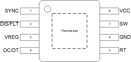
Figure 4-1 shows the UCC25800-Q1 pin diagram. For a detailed description of the device pins please refer to the Pin Configuration and Functions section in the UCC25800-Q1 data sheet.
 Figure 4-1 Pin Diagram
Following are the assumptions of use and the device configuration assumed for the pin FMA in this section: The UCC25800-Q1 is connected based on UCC25800-Q1 EVM schematic, shown in Figure 3-1 of the User's Guide.
- SYNC pin is connected with 51-Ω to GND
- No external signal source applied to SYNC pin
- DIS/FLT pin is floating
- Thermal Pad is shorted to GND
| Pin Name | Pin No. | Description of Potential Failure Effect(s) | Failure Effect Class |
|---|---|---|---|
| SYNC | 1 | Normal operation with programmed frequency. | D |
| DIS/FLT | 2 | Device is disabled. No operation. | B |
| VREG | 3 | Device is disabled. No operation. | B |
| OC/DT | 4 | Device is disabled. No operation. | B |
| RT | 5 | Device is disabled. No operation. | B |
| GND | 6 | No effect. | D |
| SW | 7 | OCP2 triggered. Possible device damage. | A |
| VCC | 8 | Device is not biased. No operation. | B |
| Pin Name | Pin No. | Description of Potential Failure Effect(s) | Failure Effect Class |
|---|---|---|---|
| SYNC | 1 | No effect. | D |
| DIS/FLT | 2 | No effect. | D |
| VREG | 3 | VREG open protection. No operation. | B |
| OC/DT | 4 | OC/DT open protection. No operation. | B |
| RT | 5 | Converter operates with 1.2-MHz switching frequency. | C |
| GND | 6 | No operation. Possible device damage | D |
| SW | 7 | Device operates normally. But converter has no output. | B |
| VCC | 8 | Device is not biased. No operation. | B |
| Pin Name | Pin No. | Shorted to | Description of Potential Failure Effect(s) | Failure Effect Class |
|---|---|---|---|---|
| SYNC | 1 | DIS/FLT | Device is disabled. No operation. | B |
| DIS/FLT | 2 | VREG | No effect. | D |
| VREG | 3 | OC/DT | Device is disabled. No operation. | B |
| OC/DT | 4 | N/A | N/A | N/A |
| RT | 5 | GND | Device is disabled. No operation. | B |
| GND | 6 | SW | OCP2 triggered. Possible device damage. | A |
| SW | 7 | VCC | OCP2 triggered. Possible device damage. | A |
| VCC | 8 | N/A | N/A | N/A |
| Pin Name | Pin No. | Description of Potential Failure Effect(s) | Failure Effect Class |
|---|---|---|---|
| SYNC | 1 | Possible device damage. | A |
| DIS/FLT | 2 | Possible device damage. | A |
| VREG | 3 | Possible device damage. | A |
| OC/DT | 4 | Possible device damage. | A |
| RT | 5 | Possible device damage. | A |
| GND | 6 | Device is not biased. No operation. | B |
| SW | 7 | OCP2 triggered. Possible device damage. | A |
| VCC | 8 | No effect. | D |