SCEA103 March 2021 SN74LXC8T245 , SN74LXC8T245-Q1 , SN74LXCH8T245
Application Brief
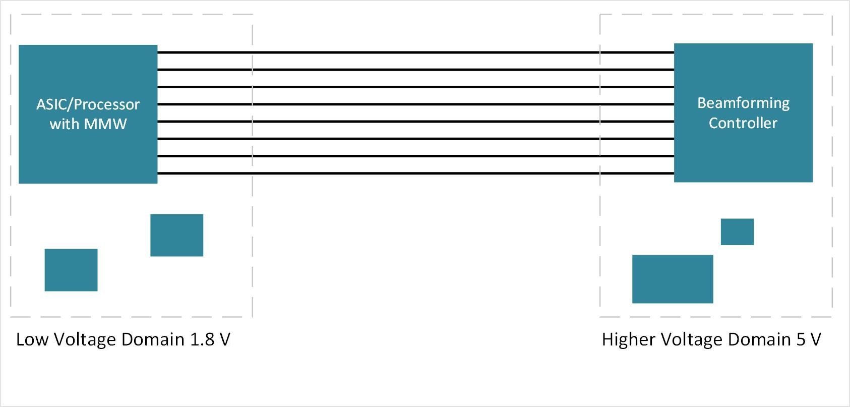
The deployment of 5G wireless infrastructure is expected to benefit both consumers and service providers in markets ranging from cellular broadband and 5G communication modules to enabling Industrial Internet of Things (IIOT). One of the key challenges facing 5G wireless infrastructure system designers is integrating the digital intensive Millimeter Wave (MMW) portion of a high band 5G design with the beamforming air interface portion (see Figure 1-1). The MMW signal chain components tend to be more digital-intensive and are therefore developed in CMOS process technologies operating at lower voltages common to CMOS process nodes such as 1.8 V or lower. Conversely, beamforming signal chain components, that require higher performance and higher power, are often developed in more exotic process technologies such as Silicon Germanium (SiGe), Gallium Arsenide (GaAs), or Gallium Nitride (GaN). Devices developed in these process technologies operate at higher voltage levels such as 5 V. As designers work to bring together MMW and beamforming signal chains, they are faced with the challenge of interconnecting signals that are operating on different voltage domains.
 Figure 1-1 MMW and Beamforming Subsystems on Different Voltage Domains
To help overcome the challenges of interconnecting Input and Output (IO) signals that are operating at different voltage levels between the MMW and beamforming sub systems, designers can turn to power efficient and robust level-shifter solutions. Level shifters with support up to 5 V often provide 5G system designers with not only the voltage level translation support they need but also enables robust signal integrity needed for interconnecting 5G signal chains. Selecting a voltage level translator with wide voltage range support, typically between 5 V and 1.8 V, can enable design engineers to resolve voltage level mismatch for many of the data and control signals often found in 5G systems. In addition to level translation, level shifters can also help system designers mitigate the impact of noisy signals. Functionality such as built-in Schmitt-Trigger inputs can enable designers to achieve better noise immunity and cleaner output transitions without the need to add external buffering devices which can introduce unwanted additional latency. The addition of integrated dynamic pulldowns enables some level translators to avoid undefined I/O states further helping to improve signal integrity. In addition, it is important that system designers select level translators that have been designed to ensure glitch-free power up without the need for complex power sequencing which can be critical for delay-sensitive applications such as cellular communications.
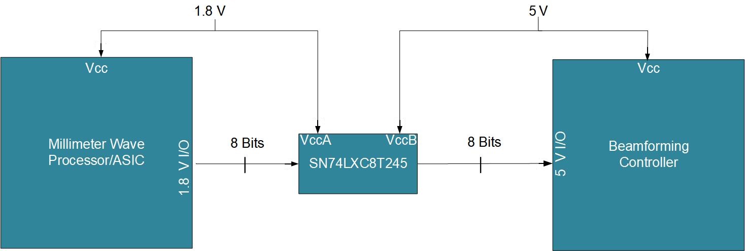
The example in Figure 1-2 shows an implementation of a 5-V to 1.8-V translator between the MMW and beamforming subsystems. In the example, the SN74LXC8T245 is used to level shift multiple control and data signals between the low voltage digital devices of the MMW signal chain and the higher voltage devices of the beamforming signal chain. Level translators like the LXC series can support level shifting for almost any 5-V to 1.1-V push-pull interface where performance, power efficiency, and robustness are paramount. For more information, see the level translation landing page at www.ti.com/translation.
 Figure 1-2 Level-Shifting Between MMW and Beamforming Signal-Chain Blocks of a 5G
System