SCDU029 December 2021 TMUX4051 , TMUX4052 , TMUX4053
4 TMUXBQB-DYYEVM Header Connections and Test Points
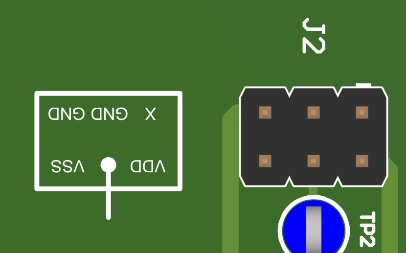
There are 16 headers located around the board with designators J1 through J16. These 3-by-2 headers serve as connections to power planes and to signals of the DUT (U1). Each pin of the DUT has similar header and test point configuration. At four different locations around the board, a legend shows the connections of the pins of the nearby five headers. Figure 4-1 shows a representation of the header associated with pin 3 of U1.
 Figure 4-1 Header J3 for U1.3
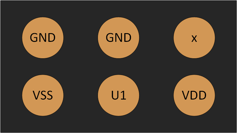
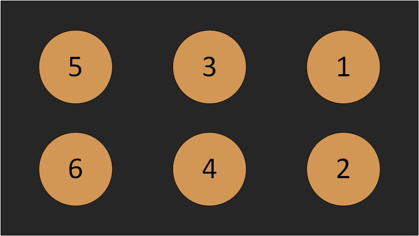
The silkscreen legend represents the connections of the pins of J2. Figure 4-2 shows the pin numbers of this header from this same perspective.

 Figure 4-2 Pinout of Headers
Table 4-1 also shows the connections.
| Header pin number | Connection |
|---|---|
| 1 | No connection |
| 2 | VDD |
| 3 | GND |
| 4 | U1 |
| 5 | GND |
| 6 | VSS |
For all headers J1 through J16, the connections are the same, but are rotated by a multiple of 90° according to their position on the board. A legend is included for each rotation.
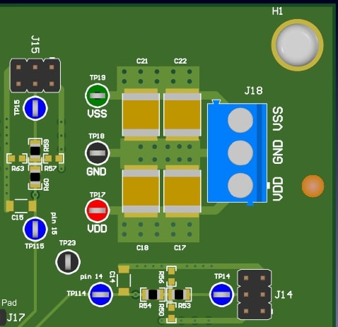
In addition to headers, multiple test points are located around the board. Black test points (TP18 and TP20-TP26) are connected to GND, the red test point (TP17) is connected to VDD, and the green test point (TP19) is connected to VSS. The remaining blue test points (TP1-TP16 and TP101-TP116) are connected along the signal paths of the pins of U1.
 Figure 4-3 Test Point Colors
Table 4-2 shows the test point connections.
| Designator | Connection |
|---|---|
| TP1 | J1.4 |
| TP2 | J2.4 |
| TP3 | J3.4 |
| TP4 | J4.4 |
| TP5 | J5.4 |
| TP6 | J6.4 |
| TP7 | J7.4 |
| TP8 | J8.4 |
| TP9 | J9.4 |
| TP10 | J10.4 |
| TP11 | J11.4 |
| TP12 | J12.4 |
| TP13 | J13.4 |
| TP14 | J14.4 |
| TP15 | J15.4 |
| TP16 | J16.4 |
| TP17 | VDD |
| TP18 | GND |
| TP19 | VSS |
| TP20 | GND |
| TP21 | GND |
| TP22 | GND |
| TP23 | GND |
| TP24 | GND |
| TP25 | GND |
| TP26 | GND |
| TP101 | U1.1 |
| TP102 | U1.2 |
| TP103 | U1.3 |
| TP104 | U1.4 |
| TP105 | U1.5 |
| TP106 | U1.6 |
| TP107 | U1.7 |
| TP108 | U1.8 |
| TP109 | U1.9 |
| TP110 | U1.10 |
| TP111 | U1.11 |
| TP112 | U1.12 |
| TP113 | U1.13 |
| TP114 | U1.14 |
| TP115 | U1.15 |
| TP116 | U1.16 |
Terminal block J18 is the power input for the board. Three power rails (VSS, GND, and VDD) are labeled on the board’s silkscreen layer, indicating the identities of the input pins of the header. Connect the power supply rails at this terminal block to power the board.