SCDU028 August 2021
6 Setup
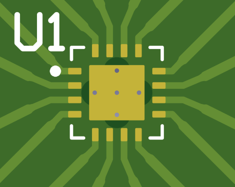
 Figure 6-1 DUT Footprint U1
The TMUXRUM-RRPEVM will not have any device connected at footprint U1, and no devices are included with the EVM for this footprint. Attach any compatible Texas Instruments 16-pin TMUX device to this location, which will serve as the Device Under Test (DUT). Compatible devices include parts with RUM or RRP package names.
By default, the TMUXRUM-RRPEVM will have shunts on headers J1 through J16 connected such that the pins of U1 are connected to GND. Remove these shunts from J1 through J16 as necessary if these connections are not desired. Alternatively, the pins of U1 can be shorted to VDD or VSS by connecting between pin 4 of the header and one of the other pins on the header. Figure 5-2 and Table 5-1 includes detailed descriptions of the connections on J1 through J16.
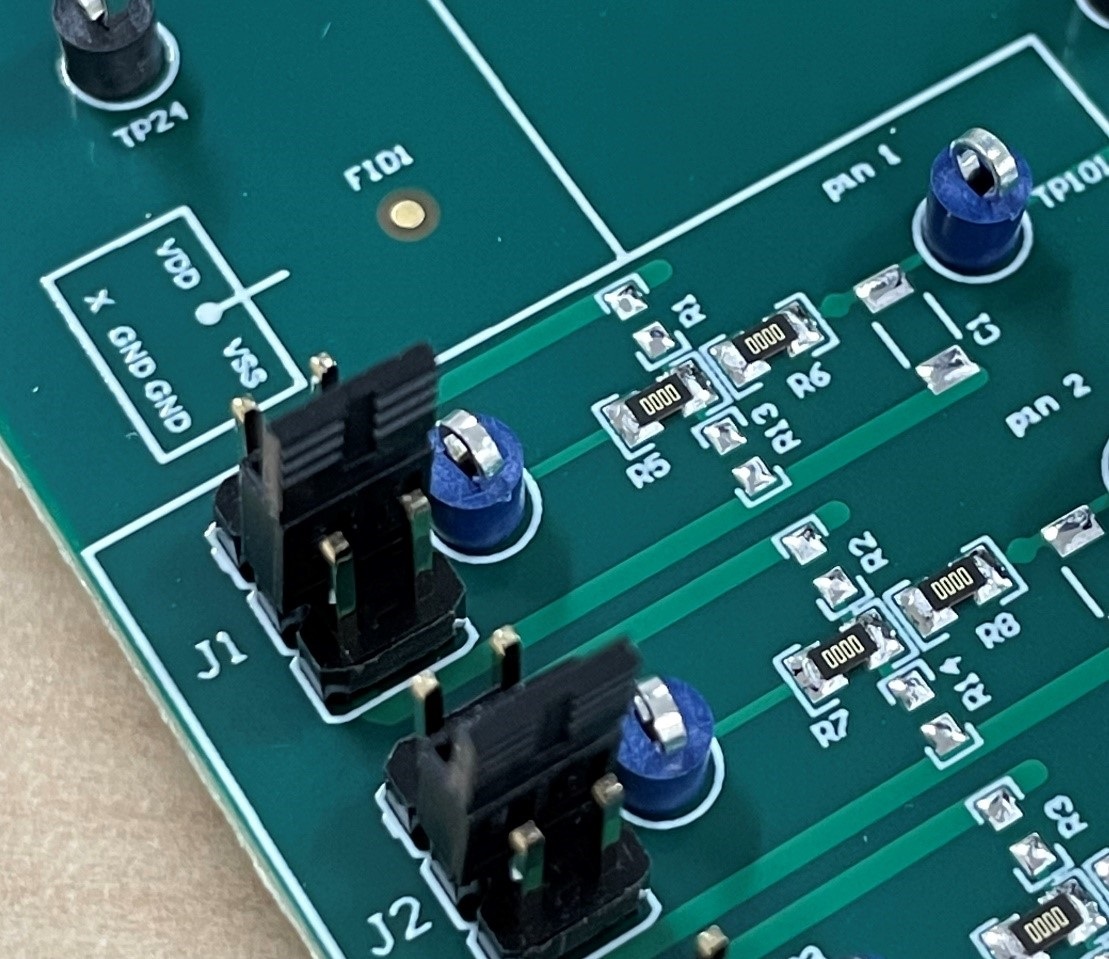
 Figure 6-2 Signal Line Circuitry (3D)
As shown in Figure 6-2 and Figure 6-3 as R5 and R6 on the J1 (pin 1 of U1) signal line, the TMUXRUM-RRPEVM includes 0 Ω series resistors (0805 package) on each signal line.
 Figure 6-3 Signal Line Circuitry
These can be substituted for different resistors as desired. Additionally, there are pads for pull-up and pull-down resistors to VDD and GND respectively. Add any 0603 resistor to the footprint shown as R1 to provide pull-up to VDD, and add any 0603 resistor to the footprint shown as R13 to provide pull-down to GND.
Each signal line also includes two footprints that allow for the user to attach capacitors or other devices with matching footprints. On the top side of the board, shown in Figure 6-2 and Figure 6-3 as C1, a standard 1206 footprint exists between the U1 pin signal and the GND signal. The user can solder a capacitor to this footprint to provide capacitance to the signal line.
 Figure 6-4 Signal Line Circuitry Bottom Layer
Figure 6-4 shows that a standard 1812 footprint exists as C101 on the backside of the board, which also allows a capacitor to be connected between the U1 pin signal and GND. The user can solder a capacitor to this footprint to provide capacitance to the signal line.
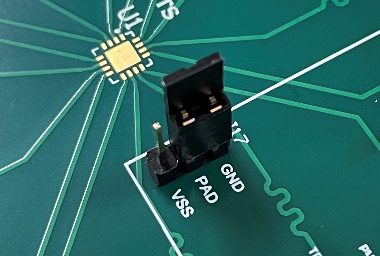
The user has the ability to select the connection of the thermal pad of U1 by using the three-by-one header located near U1 (J17).
 Figure 6-5 Thermal Pad Selector with Shunt
Connecting a shunt between pins 1 and 2 of this header will tie the thermal pad of U1 to GND, while connecting pins 2 and 3 will tie the thermal pad of U1 to VSS. Leave pin 2 of this header unconnected to allow the thermal pad to float, or use an external connection to tie the thermal pad to any other potential.