SBOU282A December 2022 – March 2023
6.2 PCB Layout
The OPA928EVM is a four-layer PCB. Figure 6-3 to Figure 6-10 show the PCB layer illustrations. The top layer consists of the configuration circuitry and output signal traces and is poured with a solid ground plane. The second layer routes the power supply connections. The third layer provides an additional layer of guard copper directly above all guard copper on the bottom layer for three-dimensional guarding. The bottom layer consists of the sensitive input traces, sensitive feedback circuitry, and guard traces and is poured with a solid ground plane. The top and bottom solder mask layers are included to show where the solder mask was removed from guard copper and RF shield mount areas.
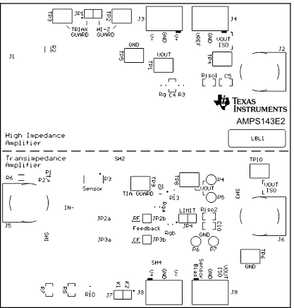 Figure 6-3 Top Overlay
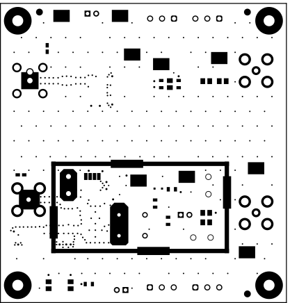 Figure 6-4 Top Solder Mask
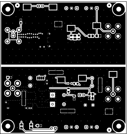 Figure 6-5 Top Layer PCB Layout
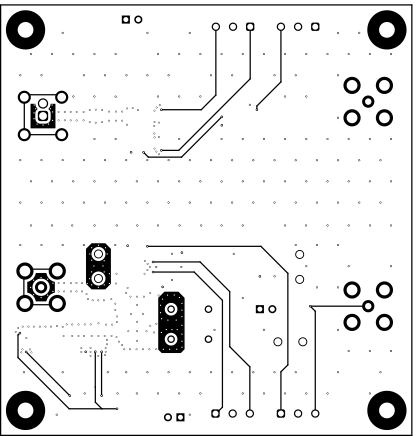 Figure 6-6 Internal Power Layer PCB
Layout
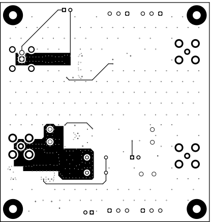 Figure 6-7 Internal Guard Layer PCB
Layout
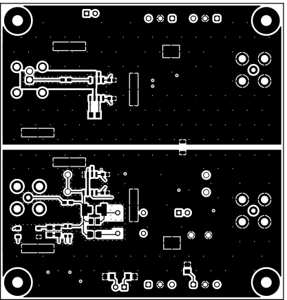 Figure 6-8 Bottom Layer PCB Layout
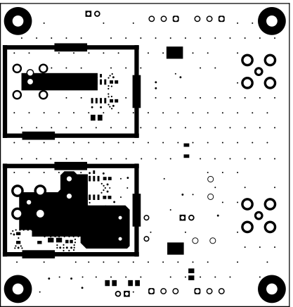 Figure 6-9 Bottom Solder Mask
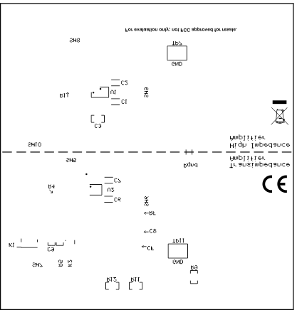 Figure 6-10 Bottom Overlay