SBOU234A December 2019 – June 2020
2.2 PCB Layout
The THP210EVM is a four-layer PCB design. Figure 2 to Figure 6 show the PCB layer illustrations.
The top layer consists of all analog signal path traces, and is poured with a solid ground plane. To minimize second and other even-harmonic content, route traces as symmetrically as possible for both positive and negative feedback pathways. Place feedback components in close proximity to the output and input pins of the device. Position decoupling capacitors C7 and C12 on the top layer as close as possible to the power-supply pins.
The second internal layer is a dedicated solid GND plane. Place independent vias at the ground connection of every component to provide a low-impedance path to ground.
The third internal layer routes the power-supply connections.
The fourth layer routes the shutdown pin and VOCM pin connections.
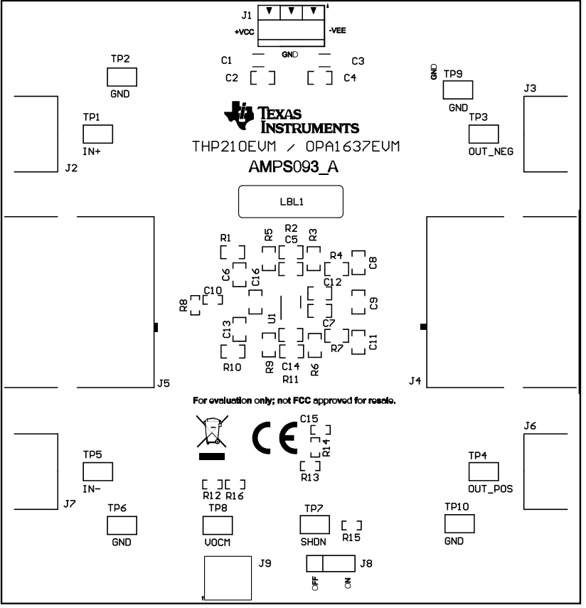 Figure 2. Top Overlay PCB Layout
 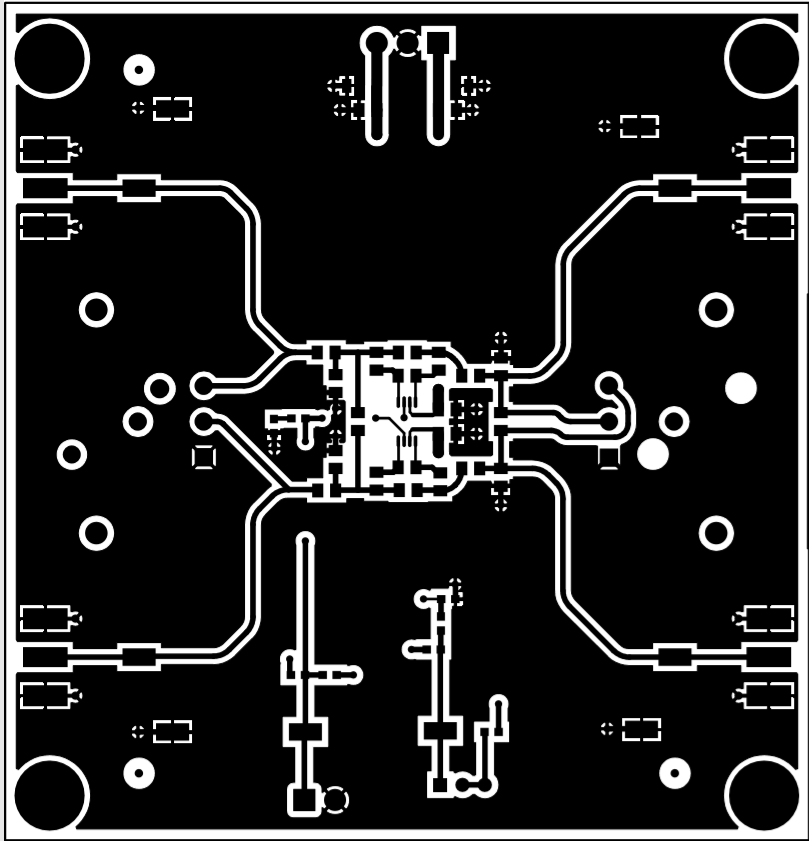 Figure 3. Top Layer PCB Layout
 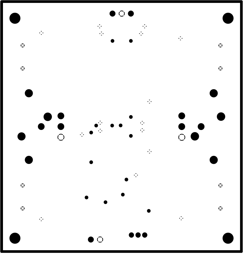 Figure 4. Ground Layer PCB Layout
 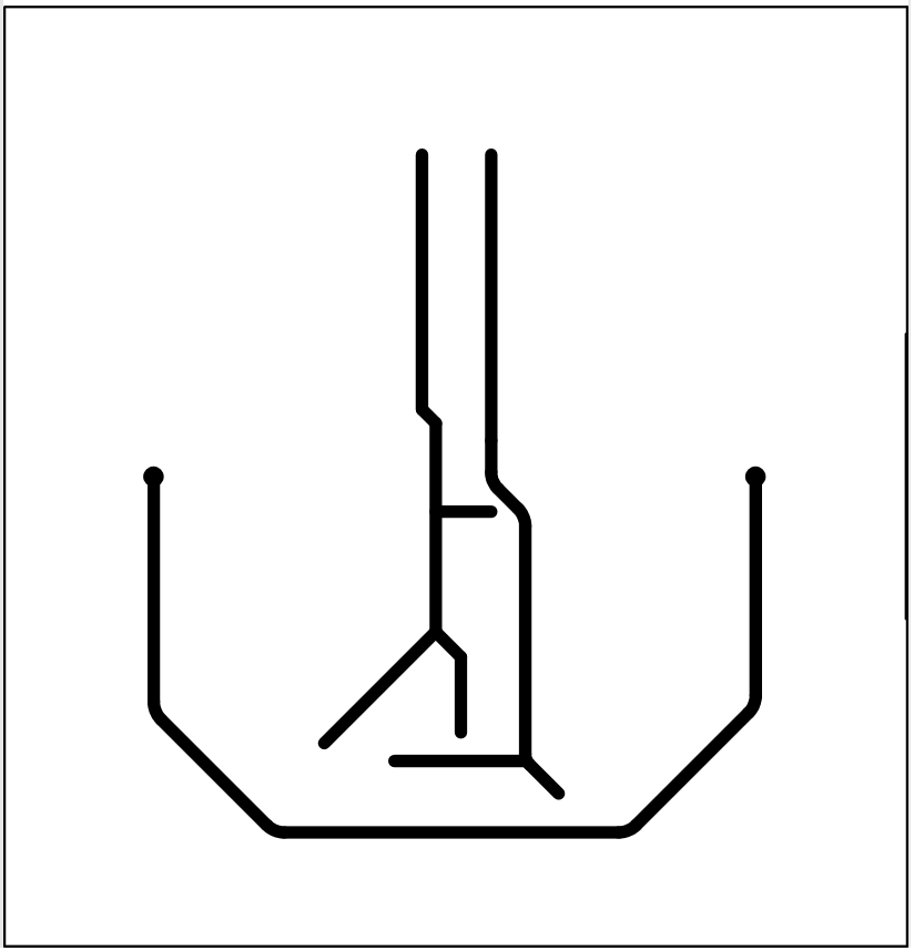 Figure 5. Power Layer PCB Layout
 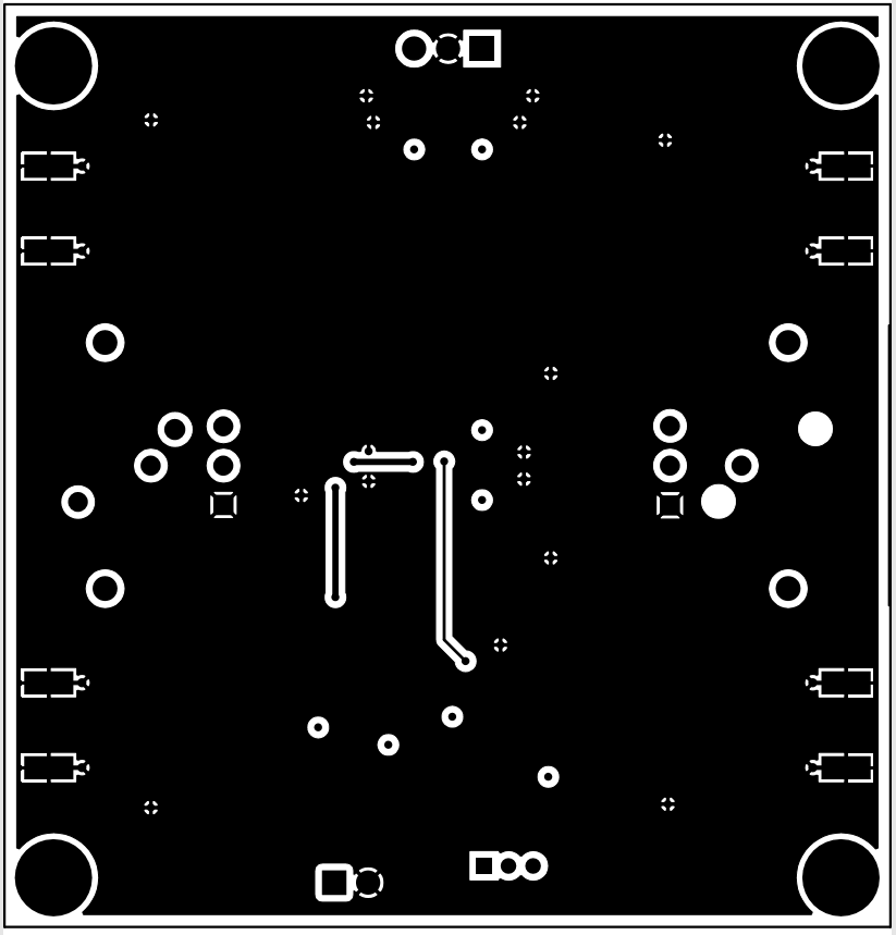 Figure 6. Bottom Layer PCB Layout