SBOA097B June 2004 – May 2015 INA132 , INA146 , INA152 , OPA2205 , OPA2277 , OPA277 , OPA301 , OPA335 , OPA364 , OPA4205 , OPA725 , TLV2341
3 Circuit 2: Single-Supply/Single-Port Approach
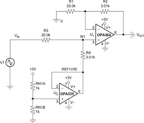
Figure 3 shows a circuit that is attractive to designers who are limited to a single low-voltage supply. The proper selection of biasing components enables both the attenuation and level-shifting functions to be accomplished in one stage.
 Figure 3. Circuit 2: Single-Supply/Single-Part
 The following series of formulas defines the relationship of the bias components:

Circuit 2 uses the following values:
- VOUT = 3V
- VIN = 20(±10)V = V1
- R1 = R3 = 20.0k 1%
- R2 = R4 = 3.01k 1%
- REF1V50 = midpoint of ADC full-scale input range.
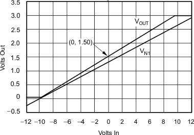
This architecture is much more compact than the modular solution of Circuit 1; however, it does rely on tight component tolerances, and does not offer either simple adjustment or filter insertion options. The DC sweep plot of Circuit 2 is shown in Figure 4. Note the large common-mode voltage swing at node N1 and the rail-to-rail output range. These two requirements make the OPA364 the best choice. Also, note the output clamping action of the OPA364, which ensures that the ADC output is not overdriven. This design can be used with input voltages far outside the power-supply rails, though designers need to pay attention to the power dissipated in R3 and the input common-mode voltage limitations of the operational amplifier.
 Figure 4. DC Sweep of Circuit 2