SBAU375 November   2021


  1.   Trademarks
  2. 1EVM Overview
    1. 1.1 Introduction
  3. 2Analog Interface
    1. 2.1 Analog Inputs
    2. 2.2 Comparator Outputs
  4. 3Power Supplies
    1. 3.1 VDD Inputs
  5. 4EVM Operation
    1. 4.1 Analog Inputs: J4
    2. 4.2 User Power: J1 and J2
    3. 4.3 Comparator Outputs: J3
    4. 4.4 Device Operation
  6. 5Layout, BOM, and Schematic
    1. 5.1 Layout
    2. 5.2 Bill of Materials (BOM)
    3. 5.3 Schematic

Layout

Figure 5-1 shows the AMC23CxxEVM PCB layout.

Note:

Board layout is not to scale. This figure is intended to show how the board is laid out, and is not intended to be used for manufacturing AMC23CxxEVM PCBs.
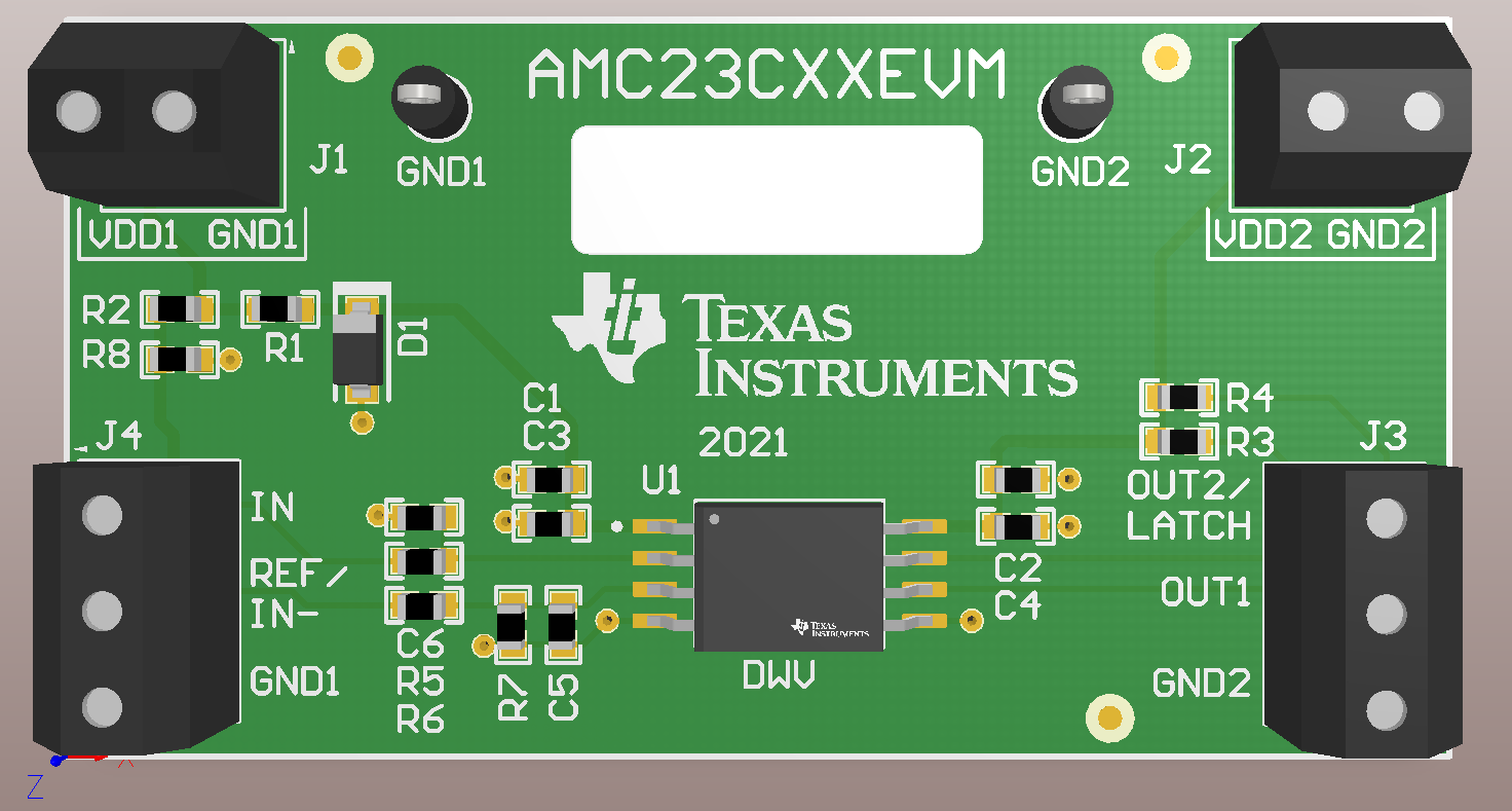
GUID-19E8CAC6-EC58-42AE-8D17-7198E02618B5-low.pngFigure 5-1 AMC23CxxEVM Top Layer Silkscreen