SNOSBI1C November 2009 – June 2015
PRODUCTION DATA.
- 1 Features
- 2 Applications
- 3 Description
- 4 Revision History
- 5 Pin Configuration and Functions
- 6 Specifications
- 7 Parameter Measurement Information
- 8 Detailed Description
-
9 Application and Implementation
- 9.1 Application Information
- 9.2
Typical Applications
- 9.2.1
8080 Interface
- 9.2.1.1 Design Requirements
- 9.2.1.2
Detailed Design Procedure
- 9.2.1.2.1 Analog Differential Voltage Inputs and Common-Mode Rejection
- 9.2.1.2.2 Analog Inputs — Input Current
- 9.2.1.2.3 Reference Voltage
- 9.2.1.2.4 Errors and Reference Voltage Adjustments
- 9.2.1.2.5 Clocking Option
- 9.2.1.2.6 Restart During a Conversion
- 9.2.1.2.7 Continuous Conversions
- 9.2.1.2.8 Driving the Data Bus
- 9.2.1.2.9 Wiring and Hook-Up Precautions
- 9.2.2 Multiple ADC0801 Series to MC6800 CPU Interface
- 9.2.3 Auto-Zeroed Differential Transducer Amplifier and ADC Converter
- 9.2.4 Multiple ADC Converters in a Z-80 Interrupt Driven Mode
- 9.2.1
8080 Interface
- 9.3 System Examples
- 10Power Supply Recommendations
- 11Layout
- 12Device and Documentation Support
- 13Mechanical, Packaging, and Orderable Information
1 Features
- Compatible With 8080-µP Derivatives – No Interfacing Logic Needed – Access Time 135 ns
- Easy Interface to All Microprocessors, or Operates as a Stand-Alone Deivce
- Differential Analog Voltage Inputs
- Logic Inputs and Outputs Meet Both MOS and TTL Voltage-Level Specifications
- Works With 2.5-V (LM336) Voltage Reference
- On-Chip Clock Generator
- 0-V to 5-V Analog Input Voltage Range With Single 5-V Supply
- No Zero Adjust Required
- 0.3-Inch Standard Width 20-Pin DIP Package
- 20-Pin Molded Chip Carrier or Small Outline Package
- Operates Ratiometrically or With 5 VDC, 2.5 VDC, or Analog Span Adjusted Voltage Reference
- Key Specifications
- Resolution: 8 Bits
- Total Error: ±1/4 LSB, ±1/2 LSB and ±1 LSB
- Conversion Time: 100 µs
2 Applications
- Operates With Any 8-Bit µP Processors or as a Stand-Alone Device
- Interface to Temp Sensors, Voltage Sources, and Transducers
3 Description
The ADC0801, ADC0802, ADC0803, ADC0804, and ADC0805 devices are CMOS 8-bit successive approximation converters (ADC) that use a differential potentiometric ladder — similar to the 256R products. These converters are designed to allow operation with the NSC800 and INS8080A derivative control bus with Tri-state output latches directly driving the data bus. These ADCs appear like memory locations or I/O ports to the microprocessor and no interfacing logic is needed.
Differential analog voltage inputs allow increasing the common-mode rejection and offsetting the analog zero input voltage value. In addition, the voltage reference input can be adjusted to allow encoding any smaller analog voltage span to the full 8 bits of resolution.
Device Information(1)
| PART NUMBER | PACKAGE | BODY SIZE (NOM) |
|---|---|---|
| ADC0801, ADC0803 | PDIP (20) | 26.073 mm × 6.604 mm |
| ADC0802, ADC0804 | PDIP (20) | 26.073 mm × 6.604 mm |
| SOIC (20) | 12.80 mm × 7.50 mm |
- For all available packages, see the orderable addendum at the end of the data sheet.
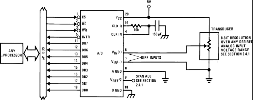
Typical Application Schematic

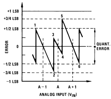
ADC0801 Specified With ±¼ LSB Accuracy
