SNOSBI1C November 2009 – June 2015
PRODUCTION DATA.
- 1 Features
- 2 Applications
- 3 Description
- 4 Revision History
- 5 Pin Configuration and Functions
- 6 Specifications
- 7 Parameter Measurement Information
- 8 Detailed Description
-
9 Application and Implementation
- 9.1 Application Information
- 9.2
Typical Applications
- 9.2.1
8080 Interface
- 9.2.1.1 Design Requirements
- 9.2.1.2
Detailed Design Procedure
- 9.2.1.2.1 Analog Differential Voltage Inputs and Common-Mode Rejection
- 9.2.1.2.2 Analog Inputs — Input Current
- 9.2.1.2.3 Reference Voltage
- 9.2.1.2.4 Errors and Reference Voltage Adjustments
- 9.2.1.2.5 Clocking Option
- 9.2.1.2.6 Restart During a Conversion
- 9.2.1.2.7 Continuous Conversions
- 9.2.1.2.8 Driving the Data Bus
- 9.2.1.2.9 Wiring and Hook-Up Precautions
- 9.2.2 Multiple ADC0801 Series to MC6800 CPU Interface
- 9.2.3 Auto-Zeroed Differential Transducer Amplifier and ADC Converter
- 9.2.4 Multiple ADC Converters in a Z-80 Interrupt Driven Mode
- 9.2.1
8080 Interface
- 9.3 System Examples
- 10Power Supply Recommendations
- 11Layout
- 12Device and Documentation Support
- 13Mechanical, Packaging, and Orderable Information
9 Application and Implementation
NOTE
Information in the following applications sections is not part of the TI component specification, and TI does not warrant its accuracy or completeness. TI’s customers are responsible for determining suitability of components for their purposes. Customers should validate and test their design implementation to confirm system functionality.
9.1 Application Information
The following sections give example circuits and suggestions for using the ADC080X in typical application situation with a typical 8-bit micro-processor.
9.1.1 Testing the ADC Converter
There are many degrees of complexity associated with testing an ADC converter. One of the simplest tests is to apply a known analog input voltage to the converter and use LEDs to display the resulting digital output code as shown in Figure 23.
For ease of testing, the VREF/2 (pin 9) should be supplied with 2.560 VDC and a VCC supply voltage of 5.12 VDC should be used. This provides an LSB value of 20 mV.
If a full-scale adjustment is to be made, an analog input voltage of 5.090 VDC (5.120–1/⁄2 LSB) should be applied to the VIN(+) pin with the VIN(−) pin grounded. The value of the VREF/2 input voltage should then be adjusted until the digital output code is just changing from 1111 1110 to 1111 1111. This value of VREF/2 should then be used for all the tests.
The digital output LED display can be decoded by dividing the 8 bits into 2 hex characters, the 4 most significant (MS) and the 4 least significant (LS). Table 1 shows the fractional binary equivalent of these two 4-bit groups. By adding the voltages obtained from the "VM" and "VLS" columns in Table 1, the nominal value of the digital display (when VREF/2 = 2.560V) can be determined. For example, for an output LED display of 1011 0110 or B6 (in hex), the voltage values from the table are 3.520 + 0.120 or 3.640 VDC. These voltage values represent the center-values of a perfect ADC converter. The effects of quantization error have to be accounted for in the interpretation of the test results.
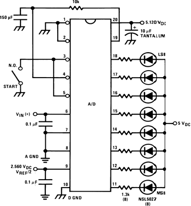 Figure 23. Basic ADC Tester
For a higher speed test system, or to obtain plotted data, a digital-to-analog converter is needed for the test set-up. An accurate 10-bit DAC can serve as the precision voltage source for the ADC. Errors of the ADC under test can be expressed as either analog voltages or differences in 2 digital words.
A basic ADC tester that uses a DAC and provides the error as an analog output voltage is shown in Figure 35. The 2 op amps can be eliminated if a lab DVM with a numerical subtraction feature is available to read the difference voltage, "A–C", directly. The analog input voltage can be supplied by a low frequency ramp generator and an X-Y plotter can be used to provide analog error (Y axis) versus analog input (X axis).
For operation with a microprocessor or a computer-based test system, it is more convenient to present the errors digitally. This can be done with the circuit of Figure 25, where the output code transitions can be detected as the 10-bit DAC is incremented. This provides 1⁄4 LSB steps for the 8-bit ADC under test. If the results of this test are automatically plotted with the analog input on the X axis and the error (in LSB’s) as the Y axis, a useful transfer function of the ADC under test results. For acceptance testing, the plot is not necessary and the testing speed can be increased by establishing internal limits on the allowed error for each code.
9.1.2 Microprocessor Interfacing
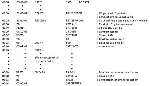
To discuss the interface with 8080A and 6800 microprocessors, a common sample subroutine structure is used. The microprocessor starts the ADC, reads and stores the results of 16 successive conversions, then returns to the user’s program. The 16 data bytes are stored in 16 successive memory locations. All Data and Addresses will be given in hexadecimal form. Software and hardware details are provided separately for each type of microprocessor.
9.1.2.1 Interfacing 8080 Microprocessor Derivatives (8048, 8085)
This converter has been designed to directly interface with derivatives of the 8080 microprocessor. The ADC can be mapped into memory space (using standard memory address decoding for CS and the MEMR and MEMW strobes) or it can be controlled as an I/O device by using the I/O R and I/O W strobes and decoding the address bits A0 → A7 (or address bits A8 → A15 as they will contain the same 8-bit address information) to obtain the CS input. Using the I/O space provides 256 additional addresses and may allow a simpler 8-bit address decoder but the data can only be input to the accumulator. To make use of the additional memory reference instructions, the ADC should be mapped into memory space. An example of an ADC in I/O space is shown in Figure 26.
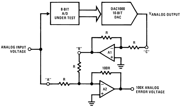 Figure 24. ADC Tester with Analog Error Output
 Figure 25. Basic “Digital” ADC Tester
Table 1. Decoding the Digital Output LEDs
| HEX | BINARY | FRACTIONAL BINARY VALUE FOR | OUTPUT VOLTAGE CENTER VALUES WITH VREF/2=2.560 VDC |
|||||||||||
|---|---|---|---|---|---|---|---|---|---|---|---|---|---|---|
| MS GROUP | LS GROUP | VMS GROUP(1) | VLS GROUP(1) | |||||||||||
| F | 1 | 1 | 1 | 1 | 15/16 | 15/256 | 4.800 | 0.300 | ||||||
| E | 1 | 1 | 1 | 0 | 7/8 | 7/128 | 4.480 | 0.280 | ||||||
| D | 1 | 1 | 0 | 1 | 13/16 | 13/256 | 4.160 | 0.260 | ||||||
| C | 1 | 1 | 0 | 0 | 3/4 | 3/64 | 3.840 | 0.240 | ||||||
| B | 1 | 0 | 1 | 1 | 11/16 | 11/256 | 3.520 | 0.220 | ||||||
| A | 1 | 0 | 1 | 0 | 5/8 | 5/128 | 3.200 | 0.200 | ||||||
| 9 | 1 | 0 | 0 | 1 | 9/16 | 9/256 | 2.880 | 0.180 | ||||||
| 8 | 1 | 0 | 0 | 0 | 1/2 | 1/32 | 2.560 | 0.160 | ||||||
| 7 | 0 | 1 | 1 | 1 | 7/16 | 7/256 | 2.240 | 0.140 | ||||||
| 6 | 0 | 1 | 1 | 0 | 3/8 | 3/128 | 1.920 | 0.120 | ||||||
| 5 | 0 | 1 | 0 | 1 | 5/16 | 2/256 | 1.600 | 0.100 | ||||||
| 4 | 0 | 1 | 0 | 0 | 1/4 | 1/64 | 1.280 | 0.080 | ||||||
| 3 | 0 | 0 | 1 | 1 | 163 | 3/256 | 0.960 | 0.060 | ||||||
| 2 | 0 | 0 | 1 | 0 | 1/8 | 1/128 | 0.640 | 0.040 | ||||||
| 1 | 0 | 0 | 0 | 1 | 1/16 | 1/256 | 0.320 | 0.020 | ||||||
| 0 | 0 | 0 | 0 | 0 | 0 | 0 | ||||||||
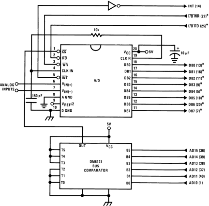
The standard control bus signals of the 8080 CS, RD and WR) can be directly wired to the digital control inputs of the ADC and the bus timing requirements are met to allow both starting the converter and outputting the data onto the data bus. A bus driver should be used for larger microprocessor systems where the data bus leaves the PCB and/or must drive capacitive loads larger than 100 pF.
9.1.2.2 Sample 8080A CPU Interfacing Circuitry and Program
The following sample program and associated hardware shown in Figure 26 may be used to input data from the converter to the INS8080A CPU chip set (comprised of the INS8080A microprocessor, the INS8228 system controller and the INS8224 clock generator). For simplicity, the ADC is controlled as an I/O device, specifically an 8-bit bi-directional port located at an arbitrarily chosen port address, E0. The Tri-state output capability of the ADC eliminates the need for a peripheral interface device, however address decoding is still required to generate the appropriate CS for the converter.
It is important to note in systems where the ADC converter is 1-of-8 or less I/O mapped devices, no address decoding circuitry is necessary. Each of the 8 address bits (A0 to A7) can be directly used as CS inputs — one for each I/O device.
9.1.2.3 INS8048 Interface
The INS8048 interface technique with the ADC0801 series (see Figure 28) is simpler than the 8080A CPU interface. There are 24 I/O lines and three test input lines in the 8048. With these extra I/O lines available, one of the I/O lines (bit 0 of port 1) is used as the chip select signal to the ADC, thus eliminating the use of an external address decoder. Bus control signals RD, WR and INT of the 8048 are tied directly to the ADC. The 16 converted data words are stored at on-chip RAM locations from 20 to 2F (Hex). The RD and WR signals are generated by reading from and writing into a dummy address, respectively. A sample interface program is shown below.
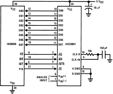 Figure 28. INS8048 Interface
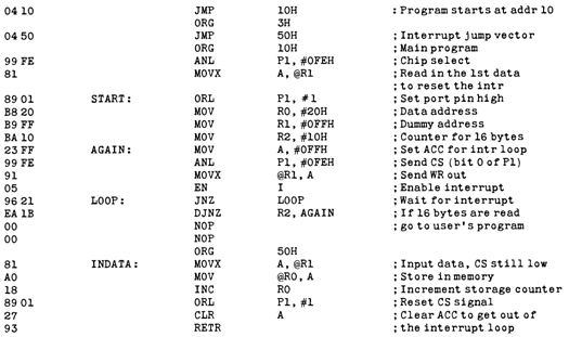 Figure 29. Sample Program for Figure 28 INS8048 Interface
9.1.2.4 Interfacing the Z-80
The Z-80 control bus is slightly different from that of the 8080. General RD and WR strobes are provided and separate memory request, MREQ, and I/O request, IORQ, signals are used which have to be combined with the generalized strobes to provide the equivalent 8080 signals. An advantage of operating the ADC in I/O space with the Z-80 is that the CPU will automatically insert one wait state (the RD and WR strobes are extended one clock period) to allow more time for the I/O devices to respond. Logic to map the ADC in I/O space is shown in Figure 30.
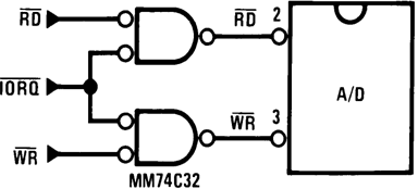 Figure 30. Mapping the ADC as an I/O Device for Use With the Z-80 CPU
Additional I/O advantages exist as software DMA routines are available and use can be made of the output data transfer which exists on the upper 8 address lines (A8 to A15) during I/O input instructions. For example, MUX channel selection for the ADC can be accomplished with this operating mode.
9.1.2.5 Interfacing 6800 Microprocessor Derivatives (6502, etc.)
The control bus for the 6800 microprocessor derivatives does not use the RD and WR strobe signals. Instead it employs a single R/W line and additional timing, if needed, can be derived from the φ2 clock. All I/O devices are memory mapped in the 6800 system, and a special signal, VMA, indicates that the current address is valid. Figure 36 shows an interface schematic where the ADC is memory mapped in the 6800 system. For simplicity, the CS decoding is shown using 1/2 DM8092. Note in many 6800 systems, an already decoded 4/5 line is brought out to the common bus at pin 21. This can be tied directly to the CS pin of the ADC, provided that no other devices are addressed at HX ADDR: 4XXX or 5XXX.
The following subroutine performs essentially the same function as in the case of the 8080A interface and it can be called from anywhere in the user’s program.
In Figure 38 the ADC0801 series is interfaced to the M6800 microprocessor through (the arbitrarily chosen) Port B of the MC6820 or MC6821 Peripheral Interface Adapter, (PIA).
Here the CS pin of the ADC is grounded because the PIA is already memory mapped in the M6800 system and no CS decoding is necessary. Also notice that the ADC output data lines are connected to the microprocessor bus under program control through the PIA and therefore the ADC RD pin can be grounded.
A sample interface program equivalent to the previous one is shown below Figure 38. The PIA Data and Control Registers of Port B are located at HEX addresses 8006 and 8007, respectively.
9.2 Typical Applications
9.2.1 8080 Interface
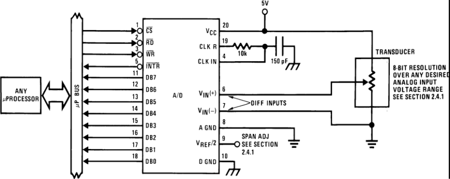
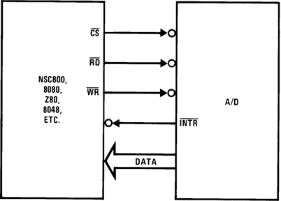 Figure 31. Generic Interface Between ADC and 8-Bit µPs
| ERROR SPECIFICATION (Includes Full-Scale, Zero Error, and Non-Linearity) | |||
|---|---|---|---|
| PART NUMBER | FULL-SCALE ADJUSTED | VREF/2 = 2.500 VDC
(No Adjustments) |
VREF/2 = No Connection (No Adjustments) |
| ADC0801 | ±1⁄4 LSB | ||
| ADC0802 | ±1⁄2 LSB | ||
| ADC0803 | ±1⁄2 LSB | ||
| ADC0804 | ±1 LSB | ||
| ADC0805 | ±1 LSB | ||
9.2.1.1 Design Requirements
For these example applications, the input analog signal is differential to illustrate the offset and common mode reduction merits. An example of the use of an adjusted reference voltage is to accommodate a reduced span or dynamic voltage range of the analog input voltage is also depicted.
Table 2. Design Parameters
| PARAMETER | EXAMPLE VALUE | |||
|---|---|---|---|---|
| ADC clock frequency, FCLK | 640 KHz | |||
| Input source resistance, RIN | 100 Ω | |||
9.2.1.2 Detailed Design Procedure
9.2.1.2.1 Analog Differential Voltage Inputs and Common-Mode Rejection
This ADC has additional applications flexibility due to the analog differential voltage input. The VIN(−) input (pin 7) can be used to automatically subtract a fixed voltage value from the input reading (tare correction). This is also useful in 4 mA–20 mA current loop conversion. In addition, common-mode noise can be reduced by use of the differential input.
The time interval between sampling VIN(+) and VIN(−) is 4-1/2 clock periods. The maximum error voltage due to this slight time difference between the input voltage samples is given by:

where
- ∆Ve is the error voltage due to sampling delay
- VP is the peak value of the common-mode voltage
- fcm is the common-mode frequency
As an example, to keep this error to 1/4 LSB (∼5 mV) when operating with a 60 Hz common-mode frequency, fcm, and using a 640 kHz ADC clock, fCLK, would allow a peak value of the common-mode voltage, VP, which is given by:

or

which gives VP–1.9 V.
The allowed range of analog input voltages usually places more severe restrictions on input common-mode noise levels.
An analog input voltage with a reduced span and a relatively large zero offset can be handled easily by making use of the differential input (see Reference Voltage).
9.2.1.2.2 Analog Inputs — Input Current
9.2.1.2.2.1 Input Bypass Capacitors
Bypass capacitors at the inputs will average these charges and cause a DC current to flow through the output resistances of the analog signal sources. This charge pumping action is worse for continuous conversions with the VIN(+) input voltage at full-scale. For continuous conversions with a 640 kHz clock frequency with the VIN(+) input at 5V, this DC current is at a maximum of approximately 5 µA. Therefore, bypass capacitors should not be used at the analog inputs or the VREF/2 pin for high resistance sources (> 1 kΩ). If input bypass capacitors are necessary for noise filtering and high source resistance is desirable to minimize capacitor size, the detrimental effects of the voltage drop across this input resistance, which is due to the average value of the input current, can be eliminated with a full-scale adjustment while the given source resistor and input bypass capacitor are both in place. This is possible because the average value of the input current is a precise linear function of the differential input voltage.
9.2.1.2.2.2 Input Source Resistance
Large values of source resistance where an input bypass capacitor is not used, will not cause errors as the input currents settle out prior to the comparison time. If a low pass filter is required in the system, use a low valued series resistor (≤ 1 kΩ) for a passive RC section or add an op amp RC active low pass filter. For low source resistance applications, (≤ 1 kΩ), a 0.1 μF bypass capacitor at the inputs will prevent noise pickup due to series lead inductance of a long wire. A 100Ω series resistor can be used to isolate this capacitor — both the R and C are placed outside the feedback loop — from the output of an op amp, if used.
9.2.1.2.2.3 Noise
The leads to the analog inputs (pins 6 and 7) should be kept as short as possible to minimize input noise coupling. Both noise and undesired digital clock coupling to these inputs can cause system errors. The source resistance for these inputs should, in general, be kept below 5 kΩ. Larger values of source resistance can cause undesired system noise pickup. Input bypass capacitors, placed from the analog inputs to ground, will eliminate system noise pickup but can create analog scale errors as these capacitors will average the transient input switching currents of the ADC (see Analog Inputs — Input Current). This scale error depends on both a large source resistance and the use of an input bypass capacitor. This error can be eliminated by doing a full-scale adjustment of the ADC (adjust VREF/2 for a proper full-scale reading — see Full-Scale) with the source resistance and input bypass capacitor in place.
Noise spikes on the VCC supply line can cause conversion errors as the comparator will respond to this noise. A low inductance tantalum filter capacitor should be used close to the converter VCC pin and values of 1 µF or greater are recommended. If an unregulated voltage is available in the system, a separate LM340LAZ-5.0, TO-92, 5-V voltage regulator for the converter (and other analog circuitry) will greatly reduce digital noise on the VCC supply.
9.2.1.2.3 Reference Voltage
9.2.1.2.3.1 Span Adjust
For maximum applications flexibility, these ADCs have been designed to accommodate a 5 VDC, 2.5 VDC or an adjusted voltage reference. This has been achieved in the design of the IC as shown in Figure 32.
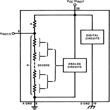 Figure 32. The VREFERENCE Design on the IC
Notice that the reference voltage for the IC is either 1/2 of the voltage applied to the VCC supply pin, or is equal to the voltage that is externally forced at the VREF/2 pin. This allows for a ratiometric voltage reference using the VCC supply, a 5 VDC reference voltage can be used for the VCC supply or a voltage less than 2.5 VDC can be applied to the VREF/2 input for increased application flexibility. The internal gain to the VREF/2 input is 2, making the full-scale differential input voltage twice the voltage at pin 9.
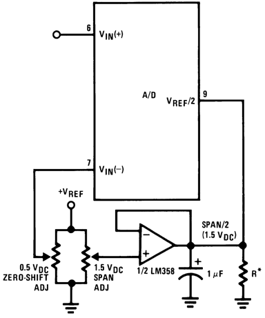
An example of the use of an adjusted reference voltage is to accommodate a reduced span — or dynamic voltage range of the analog input voltage. If the analog input voltage were to range from 0.5 VDC to 3.5 VDC, instead of 0V to 5 VDC, the span would be 3 V as shown in Figure 33. With 0.5 VDC applied to the VIN(−) pin to absorb the offset, the reference voltage can be made equal to 1/2 of the 3V span or 1.5 VDC. The ADC now will encode the VIN(+) signal from 0.5V to 3.5 V with the 0.5V input corresponding to zero and the 3.5 VDC input corresponding to full-scale. The full 8 bits of resolution are therefore applied over this reduced analog input voltage range.
9.2.1.2.3.2 Reference Accuracy Requirements
The converter can be operated in a ratiometric mode or an absolute mode. In ratiometric converter applications, the magnitude of the reference voltage is a factor in both the output of the source transducer and the output of the ADC converter and therefore cancels out in the final digital output code. The ADC0805 is specified particularly for use in ratiometric applications with no adjustments required. In absolute conversion applications, both the initial value and the temperature stability of the reference voltage are important factors in the accuracy of the ADC converter. For VREF/2 voltages of 2.4 VDC nominal value, initial errors of ±10 mVDC will cause conversion errors of ±1 LSB due to the gain of 2 of the VREF/2 input. In reduced span applications, the initial value and the stability of the VREF/2 input voltage become even more important. For example, if the span is reduced to 2.5 V, the analog input LSB voltage value is correspondingly reduced from 20 mV (5V span) to 10 mV and 1 LSB at the VREF/2 input becomes 5 mV. As can be seen, this reduces the allowed initial tolerance of the reference voltage and requires correspondingly less absolute change with temperature variations. Note that spans smaller than 2.5 V place even tighter requirements on the initial accuracy and stability of the reference source.
In general, the magnitude of the reference voltage will require an initial adjustment. Errors due to an improper value of reference voltage appear as full-scale errors in the ADC transfer function. IC voltage regulators may be used for references if the ambient temperature changes are not excessive. The LM336B 2.5-V IC reference diode (from National Semiconductor) has a temperature stability of 1.8 mV typical (6 mV maximum) over 0°C≤TA≤+70°C. Other temperature range parts are also available.
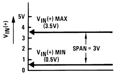 Figure 33. Analog Input Signal Example
9.2.1.2.4 Errors and Reference Voltage Adjustments
9.2.1.2.4.1 Zero Error
The zero of the ADC does not require adjustment. If the minimum analog input voltage value, VIN(MIN), is not ground, a zero offset can be done. The converter can be made to output 0000 0000 digital code for this minimum input voltage by biasing the ADC VIN(−) input at this VIN(MIN) value (see Application Information). This uses the differential mode operation of the ADC.
The zero error of the ADC converter relates to the location of the first riser of the transfer function and can be measured by grounding the VIN(−) input and applying a small magnitude positive voltage to the VIN(+) input. Zero error is the difference between the actual DC input voltage that is necessary to just cause an output digital code transition from 0000 0000 to 0000 0001 and the ideal 1/2 LSB value (1/2 LSB = 9.8 mV for VREF/2=2.500 VDC).
9.2.1.2.4.2 Full-Scale
The full-scale adjustment can be made by applying a differential input voltage that is 11/2 LSB less than the desired analog full-scale voltage range and then adjusting the magnitude of the VREF/2 input (pin 9 or the VCC supply if pin 9 is not used) for a digital output code that is just changing from 1111 1110 to 1111 1111.
9.2.1.2.4.3 Adjusting for an Arbitrary Analog Input Voltage Range
If the analog zero voltage of the ADC is shifted away from ground (for example, to accommodate an analog input signal that does not go to ground) this new zero reference should be properly adjusted first. A VIN(+) voltage that equals this desired zero reference plus 1/2 LSB (where the LSB is calculated for the desired analog span, 1 LSB=analog span/256) is applied to pin 6 and the zero reference voltage at pin 7 should then be adjusted to just obtain the 00HEX to 01HEX code transition.
The full-scale adjustment should then be made (with the proper VIN(−) voltage applied) by forcing a voltage to the VIN(+) input which is given by:

where
- VMAX = The high end of the analog input range
- VMIN = the low end (the offset zero) of the analog range. (Both are ground referenced.)
The VREF/2 (or VCC) voltage is then adjusted to provide a code change from FEHEX to FFHEX. This completes the adjustment procedure
9.2.1.2.5 Clocking Option
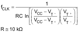
The clock for the ADC can be derived from the CPU clock or an external RC can be added to provide self-clocking. The CLK IN (pin 4) makes use of a Schmitt trigger as shown in Figure 35.
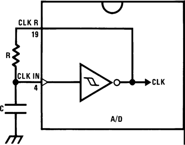 Figure 35. Self-Clocking the ADC
Heavy capacitive or DC loading of the clock R pin should be avoided as this will disturb normal converter operation. Loads less than 50 pF, such as driving up to 7 ADC converter clock inputs from a single clock R pin of 1 converter, are allowed. For larger clock line loading, a CMOS or low power TTL buffer or PNP input logic should be used to minimize the loading on the clock R pin (do not use a standard TTL buffer).
9.2.1.2.6 Restart During a Conversion
If the ADC is restarted (CS and WR go low and return high) during a conversion, the converter is reset and a new conversion is started. The output data latch is not updated if the conversion in process is not allowed to be completed, therefore the data of the previous conversion remains in this latch. The INTR output simply remains at the “1” level.
9.2.1.2.7 Continuous Conversions
For operation in the free-running mode an initializing pulse should be used, following power up, to ensure circuit operation. In this application, the CS input is grounded and the WR input is tied to the INTR output. This WR and INTR node should be momentarily forced to logic low following a power-up cycle to ensure operation.
9.2.1.2.8 Driving the Data Bus
This MOS ADC, like MOS microprocessors and memories, will require a bus driver when the total capacitance of the data bus gets large. Other circuitry, which is tied to the data bus, will add to the total capacitive loading, even in Tri-state (high impedance mode). Backplane bussing also greatly adds to the stray capacitance of the data bus.
There are some alternatives available to the designer to handle this problem. Basically, the capacitive loading of the data bus slows down the response time, even though DC specifications are still met. For systems operating with a relatively slow CPU clock frequency, more time is available in which to establish proper logic levels on the bus and therefore higher capacitive loads can be driven (see typical characteristics curves).
At higher CPU clock frequencies time can be extended for I/O reads (and/or writes) by inserting wait states (8080) or using clock extending circuits (6800).
Finally, if time is short and capacitive loading is high, external bus drivers must be used. These can be Tri-state buffers (low power Schottky such as the DM74LS240 series is recommended) or special higher drive current products which are designed as bus drivers. High current bipolar bus drivers with PNP inputs are recommended.
9.2.1.2.9 Wiring and Hook-Up Precautions
Standard digital wire wrap sockets are not satisfactory for breadboarding this ADC converter. Sockets on PCBs can be used and all logic signal wires and leads should be grouped and kept as far away as possible from the analog signal leads. Exposed leads to the analog inputs can cause undesired digital noise and hum pickup, therefore shielded leads may be necessary in many applications.
A single point analog ground that is separate from the logic ground points should be used. The power supply bypass capacitor and the self-clocking capacitor (if used) should both be returned to digital ground. Any VREF/2 bypass capacitors, analog input filter capacitors, or input signal shielding should be returned to the analog ground point. A test for proper grounding is to measure the zero error of the ADC converter. Zero errors in excess of 1/4 LSB can usually be traced to improper board layout and wiring (see Zero Error for measuring the zero error).
9.2.2 Multiple ADC0801 Series to MC6800 CPU Interface
To transfer analog data from several channels to a single microprocessor system, a multiple converter scheme presents several advantages over the conventional multiplexer single-converter approach. With the ADC0801 series, the differential inputs allow individual span adjustment for each channel. Furthermore, all analog input channels are sensed simultaneously, which essentially divides the total system servicing time of the microprocessor by the number of channels, because all conversions occur simultaneously. This scheme is shown in Figure 40.
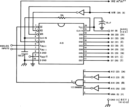
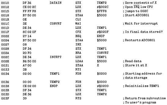
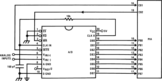 Figure 38. ADC0801–MC6820 PIA Interface
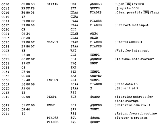 Figure 39. Sample Program for Figure 38 ADC0801–MC6820 PIA Interface
The following schematic and sample subroutine (DATA IN) in Auto-Zeroed Differential Transducer Amplifier and ADC Converter section may be used to interface (up to) 8 ADC0801’s directly to the MC6800 CPU. This scheme can easily be extended to allow the interface of more converters. In this configuration the converters are (arbitrarily) located at HEX address 5000 in the MC6800 memory space. To save components, the clock signal is derived from just one RC pair on the first converter. This output drives the other ADCs.
All the converters are started simultaneously with a STORE instruction at HEX address 5000. Note any other HEX address of the form 5XXX will be decoded by the circuit, pulling all the CS inputs low. This can easily be avoided by using a more definitive address decoding scheme. All the interrupts are ORed together to insure that all ADCs have completed their conversion before the microprocessor is interrupted.
The subroutine, DATA IN, may be called from anywhere in the user’s program. Once called, this routine initializes the CPU, starts all the converters simultaneously and waits for the interrupt signal. Upon receiving the interrupt, it reads the converters (from HEX addresses 5000 through 5007) and stores the data successively at (arbitrarily chosen) HEX addresses 0200 to 0207, before returning to the user’s pro- gram. All CPU registers then recover the original data they had before servicing DATA IN.
9.2.3 Auto-Zeroed Differential Transducer Amplifier and ADC Converter
The differential inputs of the ADC0801 series eliminate the need to perform a differential to single ended conversion for a differential transducer. Thus, one op amp can be eliminated because the differential to single ended conversion is provided by the differential input of the ADC0801 series. In general, a transducer preamp is required to take advantage of the full ADC converter input dynamic range.
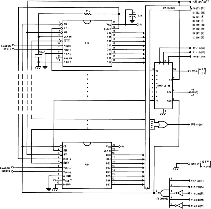
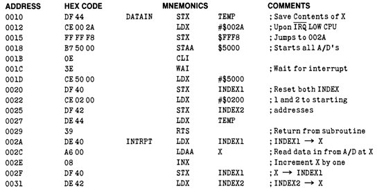 Figure 41. Sample Program for Figure 40 Interfacing Multiple ADC’s in an MC6800 System
 Figure 42. Sample Program for Figure 40 Interfacing Multiple ADC’s in an MC6800 System
Note: In order for the microprocessor to service subroutines and interrupts, the stack pointer must be dimensioned in the user’s program.
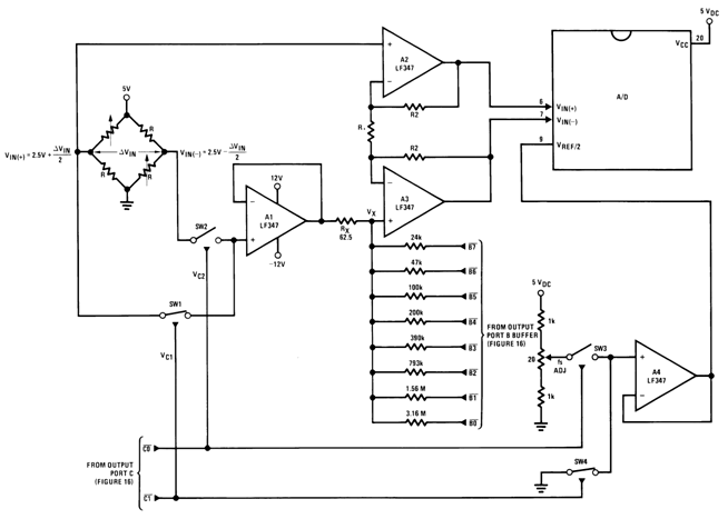
For amplification of DC input signals, a major system error is the input offset voltage of the amplifiers used for the preamp. Figure 43 is a gain of 100 differential preamp whose offset voltage errors will be cancelled by a zeroing subroutine which is performed by the INS8080A microprocessor system. The total allowable input offset voltage error for this preamp is only 50 µV for /⁄4 LSB error. This would obviously require very precise amplifiers. The expression for the differential output voltage of the preamp is:

where
- IX is the current through resistor RX
All of the offset error terms can be cancelled by making ±IXRX= VOS1 + VOS3 − VOS2. This is the principle of this auto-zeroing scheme.
The INS8080A uses the 3 I/O ports of an INS8255 Programable Peripheral Interface (PPI) to control the auto zeroing and input data from the ADC0801 as shown in Figure 44. The PPI is programmed for basic I/O operation (mode 0) with Port A being an input port and Ports B and C being output ports. Two bits of Port C are used to alternately open or close the 2 switches at the input of the preamp. Switch SW1 is closed to force the preamp’s differential input to be zero during the zeroing subroutine and then opened and SW2 is then closed for conversion of the actual differential input signal. Using 2 switches in this manner eliminates concern for the ON resistance of the switches as they must conduct only the input bias current of the input amplifiers.
Output Port B is used as a successive approximation register by the 8080 and the binary scaled resistors in series with each output bit create a D/A converter. During the zeroing subroutine, the voltage at Vx increases or decreases as required to make the differential output voltage equal to zero. This is accomplished by ensuring that the voltage at the output of A1 is approximately 2.5V so that a logic "1" (5V) on any output of Port B will source current into node VX thus raising the voltage at VX and making the output differential more negative. Conversely, a logic "0" (0V) will pull current out of node VX and decrease the voltage, causing the differential output to become more positive. For the resistor values shown, VX can move ±12 mV with a resolution of 50 µV, which will null the offset error term to /⁄4 LSB of full-scale for the ADC0801. It is important that the voltage levels that drive the auto-zero resistors be constant. Also, for symmetry, a logic swing of 0V to 5V is convenient. To achieve this, a CMOS buffer is used for the logic output signals of Port B and this CMOS package is powered with a stable 5V source. Buffer amplifier A1 is necessary so that it can source or sink the D/A output current.
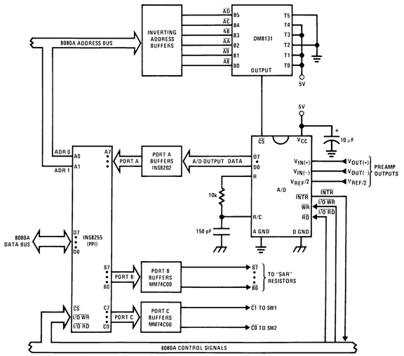 Figure 44. Microprocessor Interface Circuitry for Differential Preamp
A flow chart for the zeroing subroutine is shown in Figure 45. It must be noted that the ADC0801 series will output an all zero code when it converts a negative input [VIN(−) ≥ VIN(+)]. Also, a logic inversion exists as all of the I/O ports are buffered with inverting gates.
Basically, if the data read is zero, the differential output voltage is negative, so a bit in Port B is cleared to pull VX more negative which will make the output more positive for the next conversion. If the data read is not zero, the output voltage is positive so a bit in Port B is set to make VX more positive and the output more negative. This continues for 8 approximations and the differential output eventually converges to within 5 mV of zero.
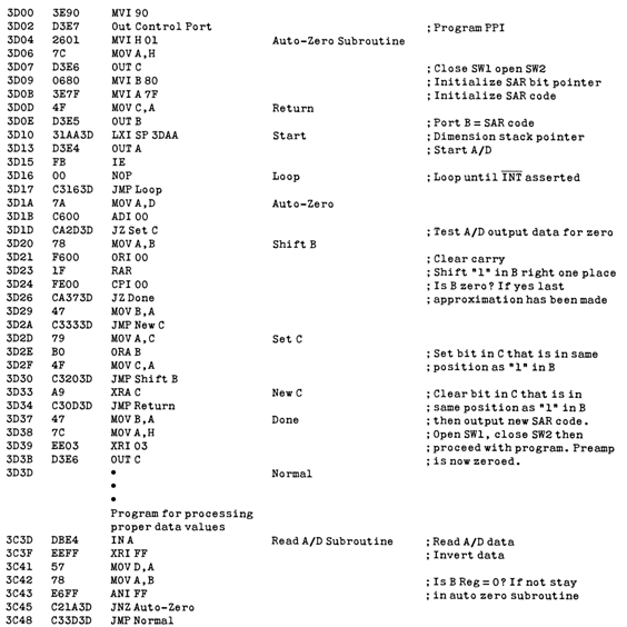
The actual program is given in Figure 46. All addresses used are compatible with the BLC 80/10 microcomputer system. In particular:
- Port A and the ADC0801 are at port address E4
- Port B is at port address E5
- Port C is at port address E6
- PPI control word port is at port address E7
- Program Counter automatically goes to ADDR:3C3D upon acknowledgment of an interrupt from the ADC0801
9.2.4 Multiple ADC Converters in a Z-80 Interrupt Driven Mode
In data acquisition systems where more than one ADC converter (or other peripheral device) will be interrupting pro- gram execution of a microprocessor, there is obviously a need for the CPU to determine which device requires servicing. Figure 47 and the accompanying software is a method of determining which of 7 ADC0801 converters has completed a conversion (INTR asserted) and is requesting an interrupt. This circuit allows starting the ADC converters in any sequence, but will input and store valid data from the converters with a priority sequence of ADC 1 being read first, ADC 2 second, etc., through ADC 7 which would have the lowest priority for data being read. Only the converters whose INT is asserted will be read.
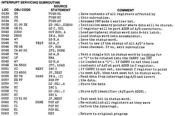
The key to decoding circuitry is the DM74LS373, 8-bit D type flip-flop. When the Z-80 acknowledges the interrupt, the program is vectored to a data input Z-80 subroutine. This subroutine will read a peripheral status word from the DM74LS373 which contains the logic state of the INTR outputs of all the converters. Each converter which initiates an interrupt will place a logic "0" in a unique bit position in the status word and the subroutine will determine the identity of the converter and execute a data read. An identifier word (which indicates which ADC the data came from) is stored in the next sequential memory location above the location of the data so the program can keep track of the identity of the data entered.
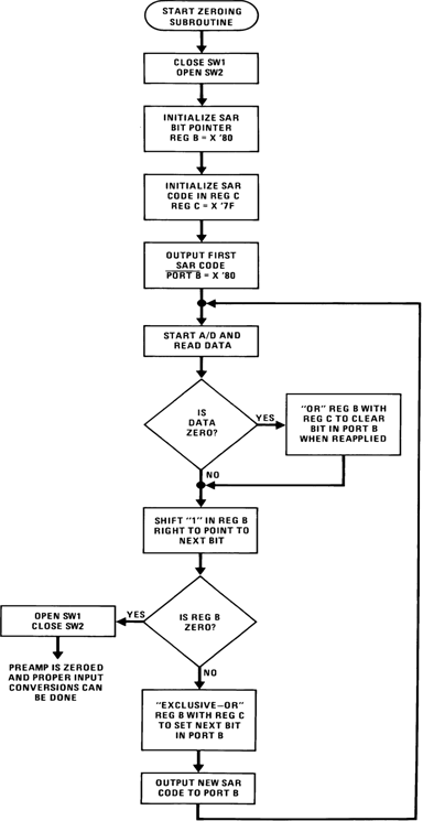 Figure 45. Flow Chart for Auto-Zero Routine
NOTE:
All numerical values are hexadecimal representations.The following notes apply:
- It is assumed that the CPU automatically performs a RST 7 instruction when a valid interrupt is acknowledged (CPU is in interrupt mode 1). Hence, the subroutine starting address of X0038.
- The address bus from the Z-80 and the data bus to the Z-80 are assumed to be inverted by bus drivers.
- ADC data and identifying words will be stored in sequential memory locations starting at the arbitrarily chosen address X 3E00.
- The stack pointer must be dimensioned in the main program as the RST 7 instruction automatically pushes the PC onto the stack and the subroutine uses an additional 6 stack addresses.
- The peripherals of concern are mapped into I/O space with the following port assignments:
Table 3. Port Assignment Where Peripherals are Mapped into I/O Space
| HEX PORT ADDRESS | PERIPHERAL | HEX PORT ADDRESS | PERIPHERAL | |
|---|---|---|---|---|
| 00 | MM74C374 8-bit flip-flop | 04 | ADC 4 | |
| 01 | ADC 1 | 05 | ADC 5 | |
| 02 | ADC 2 | 06 | ADC 6 | |
| 03 | ADC 3 | 07 | ADC 7 | |
This port address also serves as the ADC identifying word in the program.
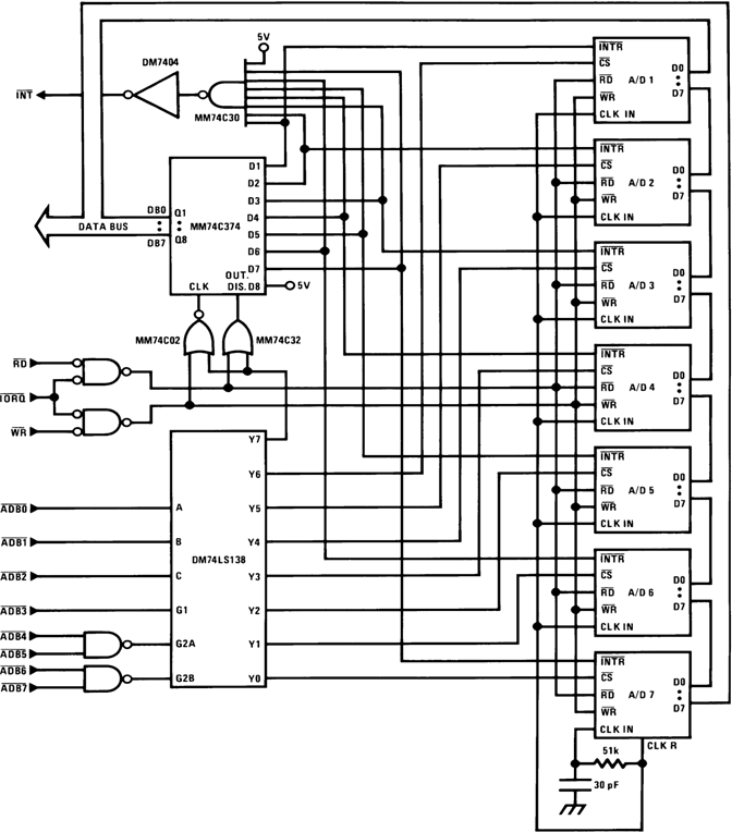 Figure 47. Multiple ADCs With Z-80 Type Microprocessor
9.3 System Examples
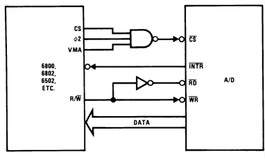 Figure 48. 6800 Interface
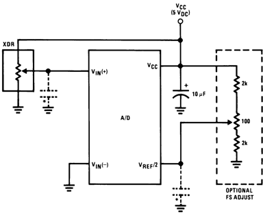
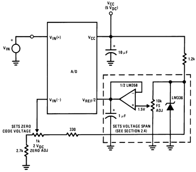 Figure 52. Zero-Shift and Span Adjust: 2 V ≤ VIN ≤ 5 V
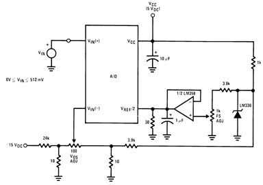
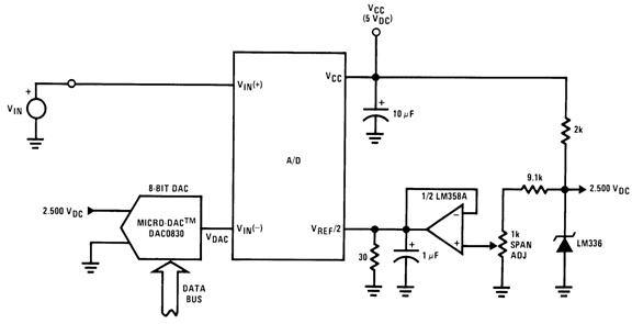
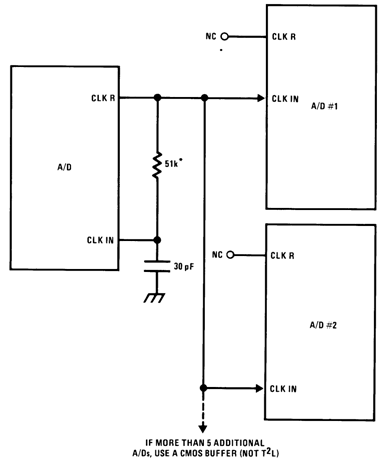
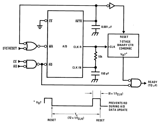 Figure 60. µP Interface for Free-Running ADC
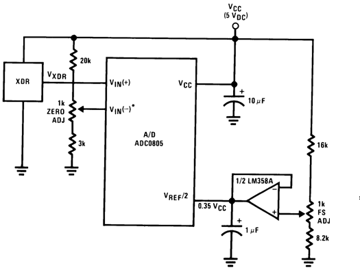
15% of VCC ≤ VXDR ≤ 85% of VCC
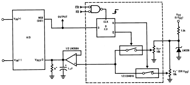
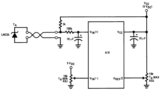 Figure 66. Low-Cost, µP-Interfaced, Temperature-to-Digital Converter
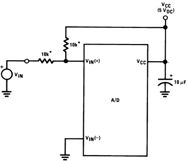
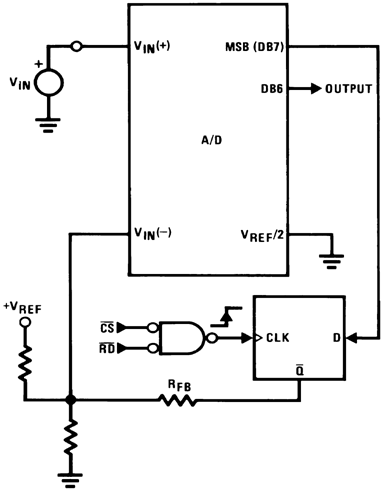 Figure 70. µP-Interfaced Comparator With Hysteresis
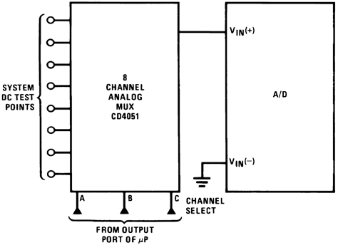 Figure 72. Analog Self-Test for a System
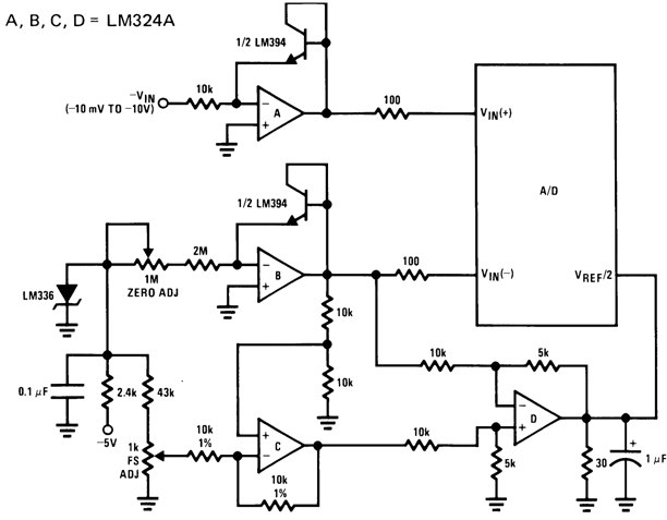
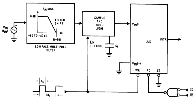
Uses Chebyshev implementation for steeper roll-off unity-gain, 2nd order, low-pass filter
Adding a separate filter for each channel increases system response time if an analog multiplexer is used
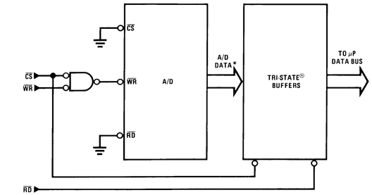
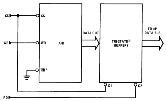
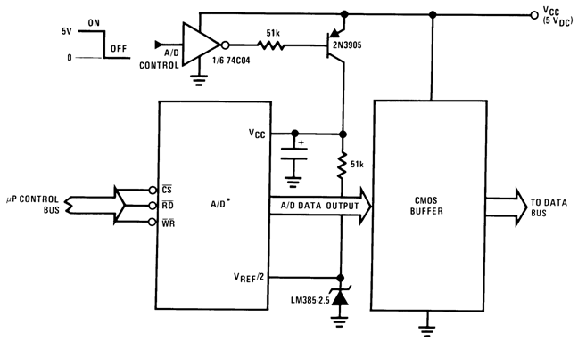
Reducing Time on Bus
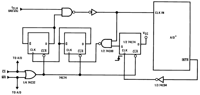
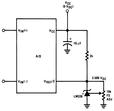
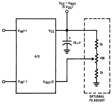 Figure 51. Absolute With a 5-V Reference
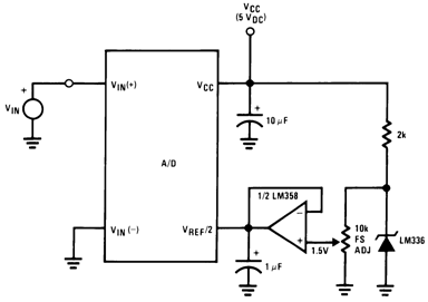 Figure 53. Span Adjust: 0 V ≤ VIN ≤ 3 V
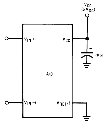
For: VIN(+) < VIN(−); Output = 00HEX
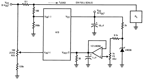 Figure 57. Digitizing a Current Flow
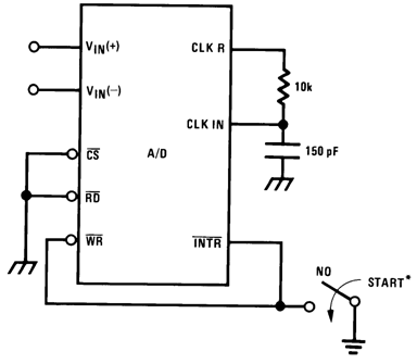
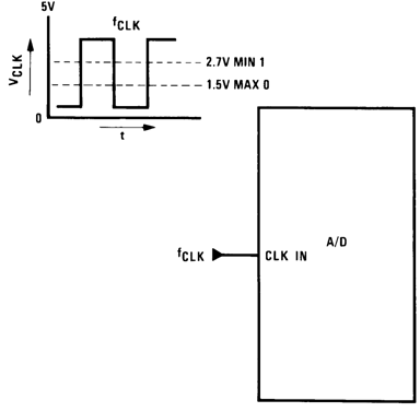
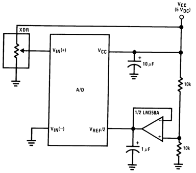 Figure 63. Ratiometric With VREF/2 Forced
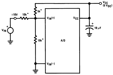
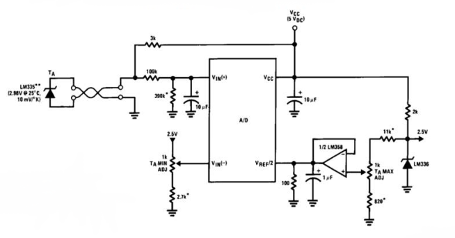
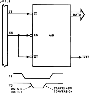 Figure 69. Read-Only Interface
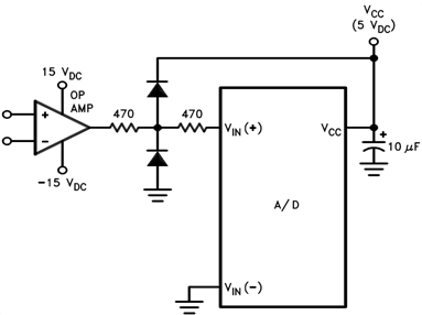
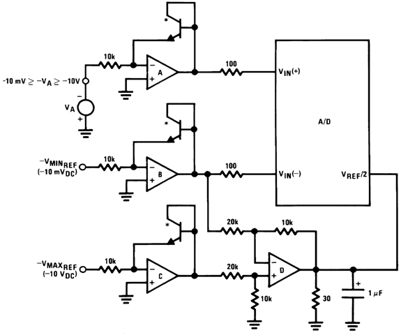
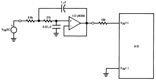 Figure 75. Noise Filtering the Analog Input
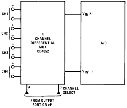 Figure 77. Multiplexing Differential Inputs
