SBOS343D September 2007 – October 2015 VCA822
PRODUCTION DATA.
- 1 Features
- 2 Applications
- 3 Description
- 4 Revision History
- 5 Device Comparison Table
- 6 Pin Configuration and Functions
-
7 Specifications
- 7.1 Absolute Maximum Ratings
- 7.2 ESD Ratings
- 7.3 Recommended Operating Conditions
- 7.4 Thermal Information
- 7.5 Electrical Characteristics: VS = ±5 V
- 7.6 Typical Characteristics: VS = ±5 V, DC Parameters
- 7.7 Typical Characteristics: VS = ±5 V, DC and Power-Supply Parameters
- 7.8 Typical Characteristics: VS = ±5 V, AVMAX = +2 V/V
- 7.9 Typical Characteristics: VS = ±5 V, AVMAX = +10 V/V
- 7.10 Typical Characteristics: VS = ±5 V, AVMAX = +100 V/V
- 8 Parameter Measurement Information
- 9 Detailed Description
-
10Application and Implementation
- 10.1 Application Information
- 10.2 Typical Applications
- 10.3 System Examples
- 11Power Supply Recommendations
- 12Layout
- 13Device and Documentation Support
- 14Mechanical, Packaging, and Orderable Information
7 Specifications
7.1 Absolute Maximum Ratings
Over operating free-air temperature range, unless otherwise noted.(1)| MIN | MAX | UNIT | ||
|---|---|---|---|---|
| Power supply | ±6.5 | V | ||
| Internal power dissipation | See Thermal Information | |||
| Input voltage | ±VS | V | ||
| Lead temperature (soldering, 10 s) | 260 | °C | ||
| Junction temperature (TJ) | 150 | °C | ||
| Junction temperature (TJ), maximum continuous operation | 140 | °C | ||
| Storage temperature | –65 | 125 | °C | |
(1) Stresses beyond those listed under Absolute Maximum Ratings may cause permanent damage to the device. These are stress ratings only, which do not imply functional operation of the device at these or any other conditions beyond those indicated under Recommended Operating Conditions. Exposure to absolute-maximum-rated conditions for extended periods may affect device reliability.
7.2 ESD Ratings
| VALUE | UNIT | |||
|---|---|---|---|---|
| V(ESD) | Electrostatic discharge | Human-body model (HBM), per ANSI/ESDA/JEDEC JS-001(1) | ±2000 | V |
| Charged-device model (CDM), per JEDEC specification JESD22-C101(2) | ±500 | |||
| Machine model (MM) | ±200 | |||
(1) JEDEC document JEP155 states that 500-V HBM allows safe manufacturing with a standard ESD control process.
(2) JEDEC document JEP157 states that 250-V CDM allows safe manufacturing with a standard ESD control process.
7.3 Recommended Operating Conditions
over operating free-air temperature range (unless otherwise noted)| MIN | NOM | MAX | UNIT | ||
|---|---|---|---|---|---|
| Operating voltage | 7 | 10 | 12 | V | |
| Operating temperature | –40 | 25 | 85 | °C | |
7.4 Thermal Information
| THERMAL METRIC(1) | VCA822 | UNIT | ||
|---|---|---|---|---|
| D [SOIC] | DGS [VSSOP] | |||
| 14 PINS | 10 PINS | |||
| RθJA | Junction-to-ambient thermal resistance | 90.3 | 173.1 | °C/W |
| RθJC(top) | Junction-to-case (top) thermal resistance | 49.8 | 46.6 | °C/W |
| RθJB | Junction-to-board thermal resistance | 44.9 | 94.3 | °C/W |
| ψJT | Junction-to-top characterization parameter | 13.8 | 2.2 | °C/W |
| ψJB | Junction-to-board characterization parameter | 44.6 | 92.7 | °C/W |
| RθJC(bot) | Junction-to-case (bottom) thermal resistance | n/a | n/a | °C/W |
(1) For more information about traditional and new thermal metrics, see the Semiconductor and IC Package Thermal Metrics application report, SPRA953.
7.5 Electrical Characteristics: VS = ±5 V
At AVMAX = +10 V/V, RF = 1 kΩ, RG = 200 Ω, and RL = 100 Ω, 25°C, unless otherwise noted.| PARAMETER | TEST CONDITIONS | MIN | TYP | MAX | UNIT | TEST LEVEL(3) | ||
|---|---|---|---|---|---|---|---|---|
| AC PERFORMANCE | ||||||||
| Small-signal bandwidth (SOIC-14 Package) | AVMAX = +2V/V, VO = 1 VPP, VG = 1 V | 168 | MHz | C | ||||
| AVMAX = +10V/V, VO = 1 VPP, VG = 1 V | 150 | MHz | C | |||||
| AVMAX = +100V/V, VO = 1 VPP, VG = 1 V | 118 | MHz | C | |||||
| Large-signal bandwidth | AVMAX = +10V/V, VO = 5VPP, VG = 1 V | 137 | MHz | C | ||||
| Gain control bandwidth | VG = 0VDC + 10 mVPP | 25°C(1) | 170 | 200 | MHz | B | ||
| 0°C to 70°C(2) | 170 | |||||||
| –40°C to +85°C(2) | 165 | |||||||
| Bandwidth for 0.1dB flatness | AVMAX = +10V/V, VO = 1VPP, VG = 1 V | 28 | MHz | C | ||||
| Slew rate | AVMAX = +10V/V, VO = 5-V Step, VG = 1 V | 25°C(1) | 1500 | 1700 | V/μs | B | ||
| 0°C to 70°C(2) | 1500 | |||||||
| –40°C to +85°C(2) | 1450 | |||||||
| Rise-and-fall time | AVMAX = +10V/V, VO = 5-V Step, VG = 1 V | 25°C(1) | 2.5 | 3.1 | ns | B | ||
| 0°C to 70°C(2) | 3.2 | |||||||
| –40°C to +85°C(2) | 3.2 | |||||||
| Settling time to 0.01% | AVMAX = +10V/V, VO = 5V Step, VG = 1 V | 11 | ns | C | ||||
| Harmonic distortion, 2nd-harmonic | VO = 2VPP, f = 20MHz, VG = 1 V | 25°C(1) | –60 | –62 | dBc | B | ||
| 0°C to 70°C(2) | –60 | |||||||
| –40°C to +85°C(2) | –60 | |||||||
| Harmonic distortion, 3rd-harmonic | VO = 2VPP, f = 20MHz, VG = 1 V | 25°C(1) | –66 | –68 | dBc | B | ||
| 0°C to 70°C(2) | –66 | |||||||
| –40°C to +85°C(2) | –66 | |||||||
| Input voltage noise | f > 100kHz, VG = 1 V | 8.2 | nV/√Hz | C | ||||
| Input current noise | f > 100kHz, VG = 1 V | 2.6 | pA/√Hz | C | ||||
| GAIN CONTROL | ||||||||
| Absolute gain error | AVMAX = +10V/V, VG = 1 V | 25°C(1) | ±0.1 | ±0.4 | dB | A | ||
| 0°C to 70°C(2) | ±0.5 | |||||||
| –40°C to +85°C(2) | ±0.6 | |||||||
| Gain deviation | AVMAX = +10V/V, 0 < VG < 1 V | 25°C(1) | ±0.05 | ±0.3 | dB | A | ||
| 0°C to 70°C(2) | ±0.34 | |||||||
| –40°C to +85°C(2) | ±0.37 | |||||||
| Gain deviation | AVMAX = +10V/V, –0.8 < VG < 1 V | 25°C(1) | ±1.06 | ±1.9 | dB | A | ||
| 0°C to 70°C(2) | ±2.1 | |||||||
| –40°C to +85°C(2) | ±2.2 | |||||||
| Gain at VG = –0.9V | Relative to maximum gain | 25°C(1) | –26 | –24 | dB | A | ||
| 0°C to 70°C(2) | –24 | |||||||
| –40°C to +85°C(2) | –23 | |||||||
| Gain control bias current | VG = 0 V | 25°C(1) | 22 | 30 | μA | A | ||
| 0°C to 70°C(2) | 35 | |||||||
| –40°C to +85°C(2) | 37 | |||||||
| Average gain control bias current drift | VG = 0 V | 0°C to 70°C(2) | ±100 | nA/°C | B | |||
| –40°C to +85°C(2) | ±100 | |||||||
| Gain control input impedance | 70 || 1 | kΩ || pF | C | |||||
| DC PERFORMANCE | ||||||||
| Input offset voltage | AVMAX = +10V/V, VCM = 0 V, VG = 0 V | 25°C(1) | ±4 | ±17 | mV | A | ||
| 0°C to 70°C(2) | ±17.8 | |||||||
| –40°C to +85°C(2) | ±19 | |||||||
| Average input offset voltage drift | AVMAX = +10V/V, VCM = 0 V, VG = 0 V | 0°C to 70°C(2) | ±30 | μV/°C | B | |||
| –40°C to +85°C(2) | ±30 | |||||||
| Input bias current | AVMAX = +10V/V, VCM = 0 V, VG = 0 V | 25°C(1) | 19 | 25 | μA | A | ||
| 0°C to 70°C(2) | 29 | |||||||
| –40°C to +85°C(2) | 31 | |||||||
| Average input bias current drift | AVMAX = +10V/V, VCM = 0 V, VG = 0 V | 0°C to 70°C(2) | ±90 | nA/°C | B | |||
| –40°C to +85°C(2) | ±90 | |||||||
| Input offset current | AVMAX = +10V/V, VCM = 0 V, VG = 0 V | 25°C(1) | ±0.5 | ±2.5 | μA | A | ||
| 0°C to 70°C(2) | ±3.2 | |||||||
| –40°C to +85°C(2) | ±3.5 | |||||||
| Average input offset current drift | AVMAX = +10V/V, VCM = 0 V, VG = 0 V | 0°C to 70°C(2) | ±16 | nA/°C | B | |||
| –40°C to +85°C(2) | ±16 | |||||||
| IRG MAX | Maximum current through gain resistance | 25°C(1) | ±2.6 | ±2.55 | mA | B | ||
| 0°C to 70°C(2) | ±2.55 | |||||||
| –40°C to +85°C(2) | ±2.5 | |||||||
| INPUT | ||||||||
| Most positive input voltage | RL = 100Ω | 25°C(1) | +1.6 | +1.6 | V | A | ||
| 0°C to 70°C(2) | +1.6 | |||||||
| –40°C to +85°C(2) | +1.6 | |||||||
| Most negative input voltage | RL = 100Ω | 25°C(1) | –2.1 | –2.1 | V | A | ||
| 0°C to 70°C(2) | –2.1 | |||||||
| –40°C to +85°C(2) | –2.1 | |||||||
| Common-mode rejection ratio | VCM = ±0.5V | 25°C(1) | 65 | 80 | dB | A | ||
| 0°C to 70°C(2) | 60 | |||||||
| –40°C to +85°C(2) | 60 | |||||||
| Input impedance, differential | 0.5 || 1 | MΩ || pF | C | |||||
| Input impedance, common-mode | 0.5 || 2 | MΩ || pF | C | |||||
| OUTPUT | ||||||||
| Output voltage swing | RL = 1kΩ | 25°C(1) | ±3.8 | ±4.0 | V | A | ||
| 0°C to 70°C(2) | ±3.75 | |||||||
| –40°C to +85°C(2) | ±3.7 | |||||||
| RL = 100Ω | 25°C(1) | ±3.7 | ±3.9 | V | A | |||
| 0°C to 70°C(2) | ±3.6 | |||||||
| –40°C to +85°C(2) | ±3.5 | |||||||
| Output current | VO = 0V, RL = 5Ω | 25°C(1) | ±140 | ±160 | mA | A | ||
| 0°C to 70°C(2) | ±130 | |||||||
| –40°C to +85°C(2) | ±130 | |||||||
| Output impedance | AVMAX = +10V/V, f > 100kHz, VG = 1V | 0.01 | Ω | C | ||||
| POWER SUPPLY | ||||||||
| Specified operating voltage | ±5 | V | C | |||||
| Minimum operating voltage | ±3.5 | V | C | |||||
| Maximum operating voltage | 25°C(1) | V | A | |||||
| 0°C to 70°C(2) | ||||||||
| –40°C to +85°C(2) | ||||||||
| Maximum quiescent current | VG = 0V | 25°C(1) | 36 | 37 | mA | A | ||
| 0°C to 70°C(2) | 37.5 | |||||||
| –40°C to +85°C(2) | 38 | |||||||
| Minimum quiescent current | VG = 0V | 25°C(1) | 36 | 34.5 | mA | A | ||
| 0°C to 70°C(2) | 34 | |||||||
| –40°C to +85°C(2) | 33.5 | |||||||
| –PSRR | Power-supply rejection ratio | VG = +1V | 25°C(1) | –61 | –68 | dB | A | |
| 0°C to 70°C(2) | –59 | |||||||
| –40°C to +85°C(2) | –58 | |||||||
| THERMAL CHARACTERISTICS | ||||||||
| Specified operating range, D package | –40 to +85 | °C | C | |||||
| θJA | Junction-to-ambient Thermal resistance | MSOP-10 (DGS) | 130 | °C/W | C | |||
| SOIC-14 (D) | 80 | °C/W | C | |||||
(1) Junction temperature = ambient for +25°C tested specifications.
(2) Junction temperature = ambient at low temperature limit; junction temperature = ambient +23°C at high temperature limit for over temperature specifications.
(3) Test levels: (A) 100% tested at 25°C. Over temperature limits set by characterization and simulation. (B) Limits set by characterization and simulation. (C) Typical value only for information.
7.6 Typical Characteristics: VS = ±5 V, DC Parameters
At TA = 25°C, RL = 100 Ω, VG = 1 V, and VIN = single-ended input on +VIN with –VIN at ground, unless otherwise noted.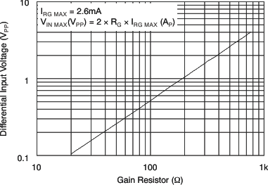 Figure 1. Maximum Differential Input Voltage vs RG
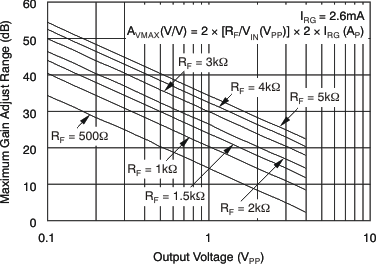 Figure 3. Maximum Gain Adjust Range vs
Peak-to-Peak Output Voltage
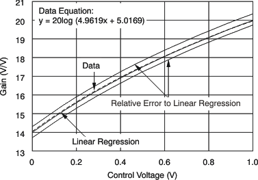 Figure 5. Gain Error Band vs
Gain Control Voltage
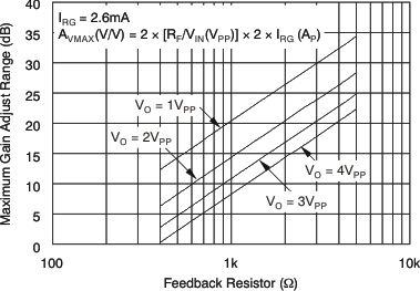 Figure 2. Maximum Gain Adjust Range vs RF
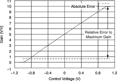 Figure 4. Gain Error Band vs
Gain Control Voltage
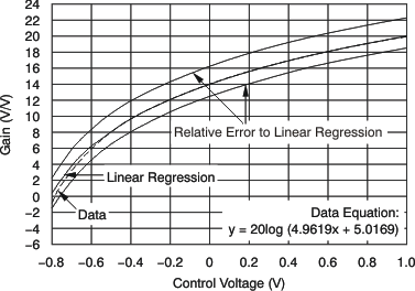 Figure 6. Gain Error Band vs
Gain Control Voltage
7.7 Typical Characteristics: VS = ±5 V, DC and Power-Supply Parameters
At TA = +25°C, RL = 100 Ω, VG = +1 V, and VIN = single-ended input on +VIN with –VIN at ground, unless otherwise noted.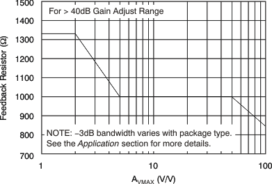 Figure 7. Recommended RF vs AVMAX
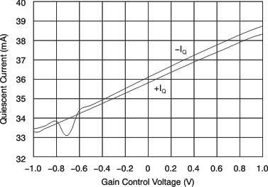 Figure 9. Supply Current vs Control Voltage
(AVMAX = +10 V/V)
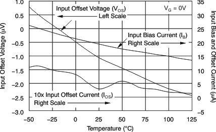 Figure 11. Typical DC Drift vs Temperature
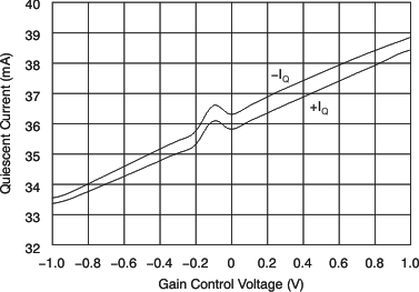 Figure 8. Supply Current vs Control Voltage
(AVMAX = +2 V/V)
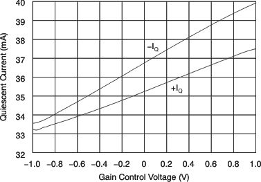 Figure 10. Supply Current vs Control Voltage
(AVMAX = +100 V/V)
7.8 Typical Characteristics: VS = ±5 V, AVMAX = +2 V/V
At TA = +25°C, RL = 100 Ω, RF = 1.33 kΩ, RG = 1.33 kΩ, VG = +1 V, VIN = single-ended input on +VIN with –VIN at ground, and SOIC-14 package, unless otherwise noted.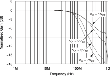 Figure 12. Large-Signal Frequency Response
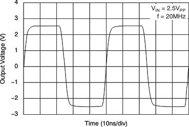 Figure 14. Large-Signal Pulse Response
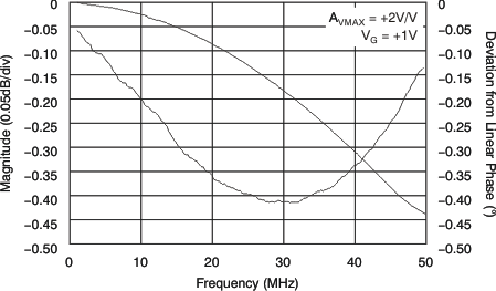
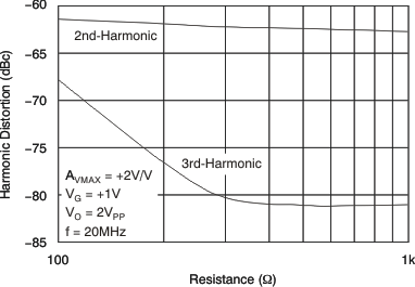 Figure 18. Harmonic Distortion vs Load Resistance
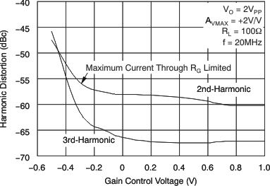 Figure 20. Harmonic Distortion vs
Gain Control Voltage
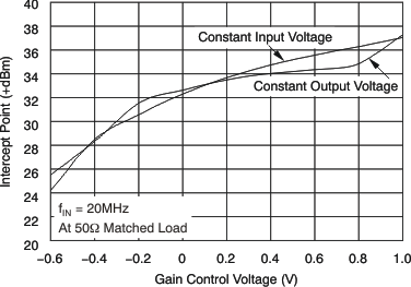 Figure 22. Two-Tone, Third-Order Intermodulation Intercept
vs Gain Control Voltage
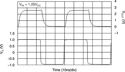 Figure 24. Gain Control Pulse Response
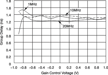 Figure 26. Group Delay vs Gain Control Voltage
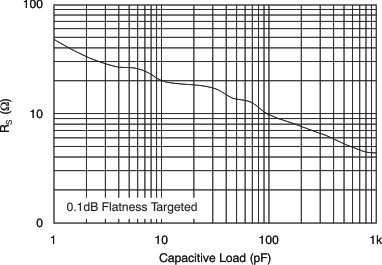 Figure 28. Recommended RS vs Capacitive Load
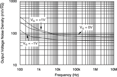 Figure 30. Output Voltage Noise Density
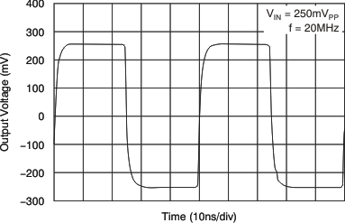 Figure 13. Small-Signal Pulse Response
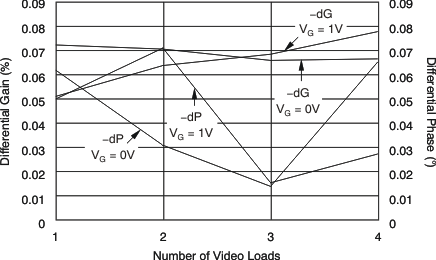 Figure 15. Composite Video dG/dP
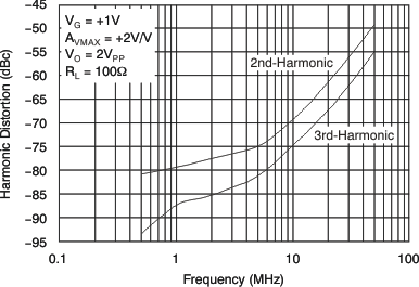 Figure 17. Harmonic Distortion vs Frequency
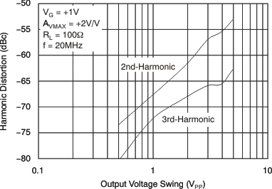 Figure 19. Harmonic Distortion vs
Output Voltage
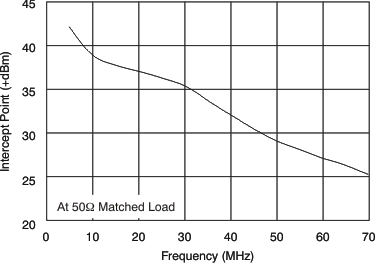 Figure 21. Two-Tone, Third-Order
Intermodulation Intercept
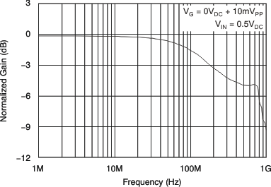 Figure 23. Gain Control Frequency Response
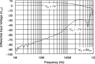 Figure 25. Fully-Attenuated Response
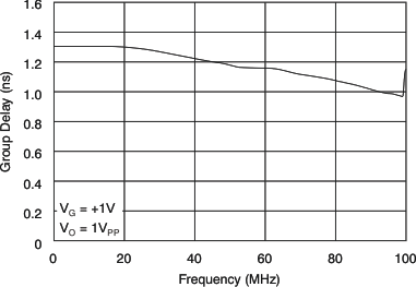 Figure 27. Group Delay vs Frequency
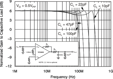 Figure 29. Frequency Response vs Capacitive Load
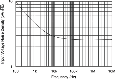 Figure 31. Input Current Noise Density
7.9 Typical Characteristics: VS = ±5 V, AVMAX = +10 V/V
At TA = +25°C, RL = 100 Ω, RF = 1 kΩ, RG = 200 Ω, VG = +1 V, and VIN = single-ended input on +VIN with –VIN at ground, unless otherwise noted.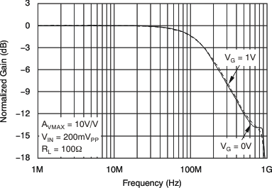 Figure 32. Small-Signal Frequency Response
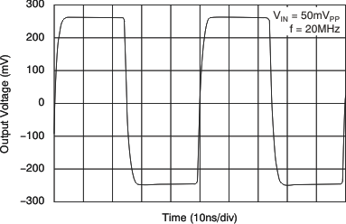 Figure 34. Small-Signal Pulse Response
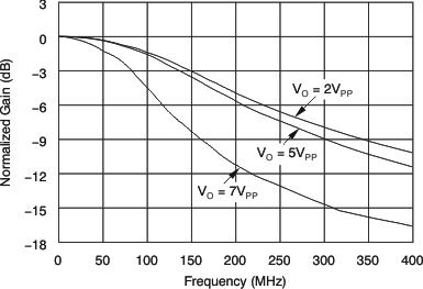 Figure 33. Large-Signal Frequency Response
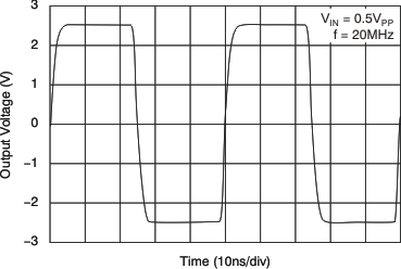 Figure 35. Large-Signal Pulse Response
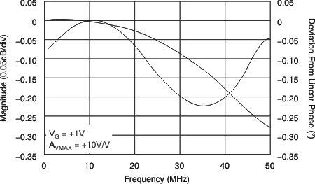 Figure 36. Gain Flatness, Deviation From Linear Phase
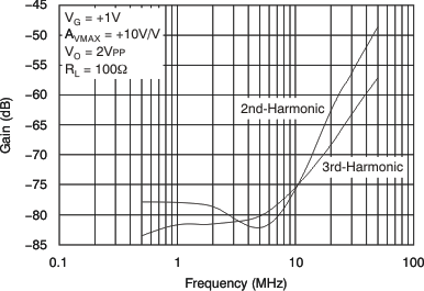 Figure 38. Harmonic Distortion vs Frequency
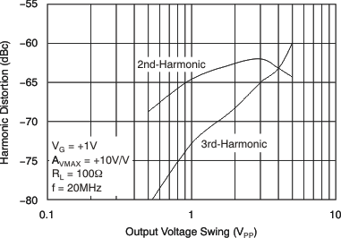 Figure 40. Harmonic Distortion vs
Output Voltage
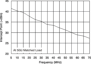 Figure 42. Two-Tone, Third-Order
Intermodulation Intercept
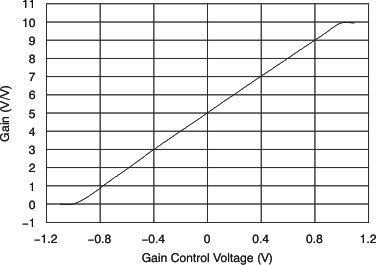 Figure 44. Gain vs Gain Control Voltage
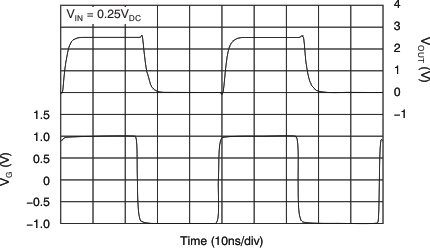 Figure 46. Gain Control Pulse Response
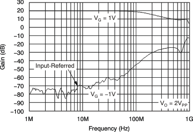 Figure 48. Fully-Attenuated Response
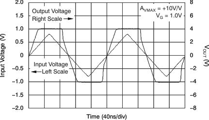 Figure 50. Output Limited Overdrive Recovery
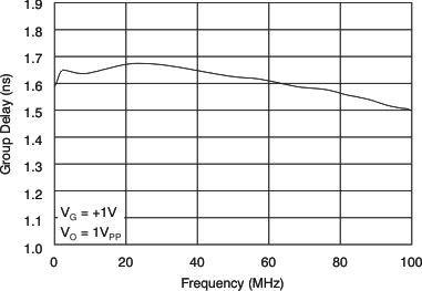 Figure 52. Group Delay vs Frequency
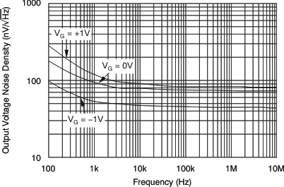 Figure 37. Output Voltage Noise Density
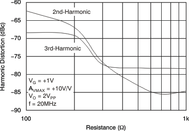 Figure 39. Harmonic Distortion vs Load Resistance
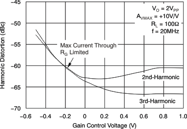 Figure 41. Harmonic Distortion vs
Gain Control Voltage
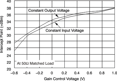 Figure 43. Two-Tone, Third-Order Intermodulation Intercept
vs Gain Control Voltage (fIN = 20 MHz)
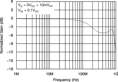 Figure 45. Gain Control Frequency Response
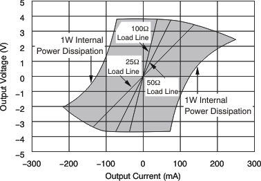 Figure 47. Output Voltage and Current Limitations
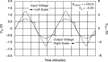 Figure 49. IRG Limited Overdrive Recovery
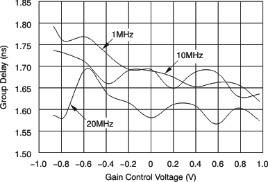 Figure 51. Group Delay vs Gain Control Voltage
7.10 Typical Characteristics: VS = ±5 V, AVMAX = +100 V/V
At TA = +25°C, RL = 100 Ω, RF = 845 Ω, RG = 16.9 Ω, VG = +1 V, VIN = single-ended input on +VIN with –VIN at ground, and SOIC-14 package, unless otherwise noted.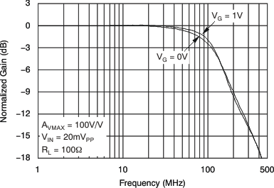 Figure 53. Small-Signal Frequency Response
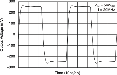 Figure 55. Small-Signal Pulse Response
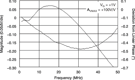 Figure 57. Gain Flatness
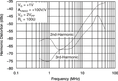 Figure 59. Harmonic Distortion vs Frequency
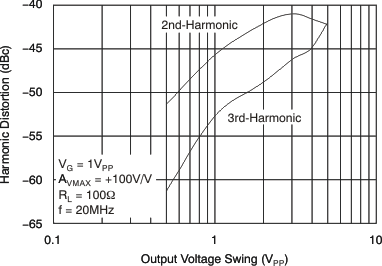 Figure 61. Harmonic Distortion vs
Output Voltage
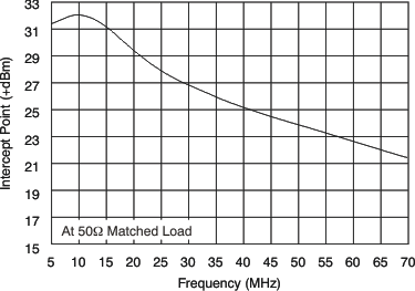 Figure 63. Two-Tone, Third-Order
Intermodulation Intercept
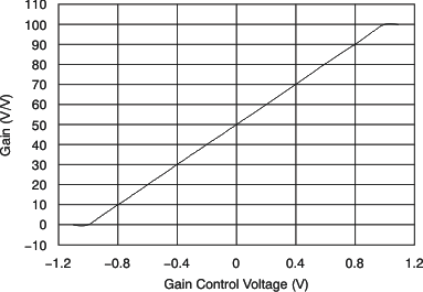 Figure 65. Gain vs Gain Control Voltage
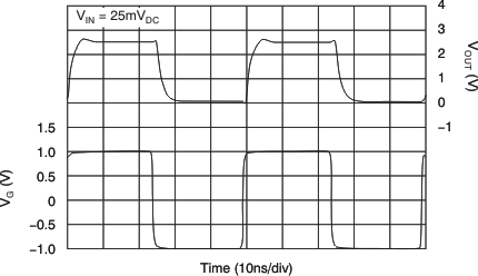 Figure 67. Gain Control Pulse Response
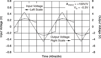 Figure 69. IRG Limited Overdrive Recovery
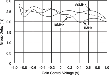 Figure 71. Group Delay vs Gain Control Voltage
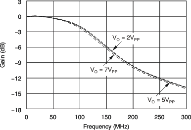 Figure 54. Large-Signal Frequency Response
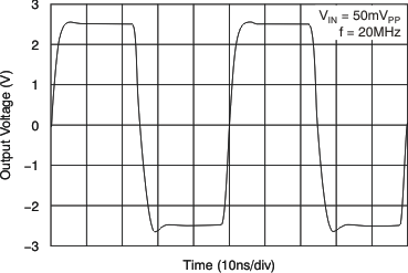 Figure 56. Large-Signal Pulse Response
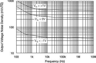 Figure 58. Output Voltage Noise Density
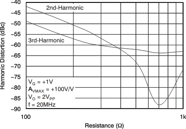 Figure 60. Harmonic Distortion vs Load Resistance
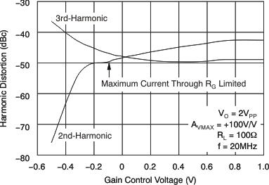 Figure 62. Harmonic Distortion vs
Gain Control Voltage
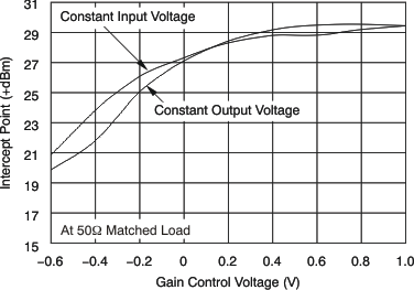 Figure 64. Two-Tone, Third-Order Intermodulation Intercept
vs Gain Control Voltage (fIN = 20 MHz)
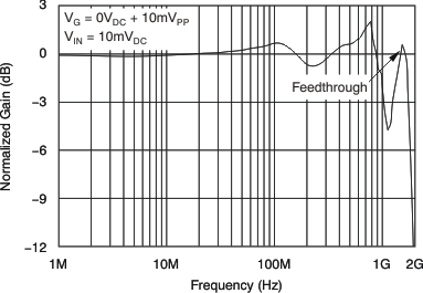 Figure 66. Gain Control Frequency Response
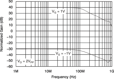 Figure 68. Fully-Attenuated Response
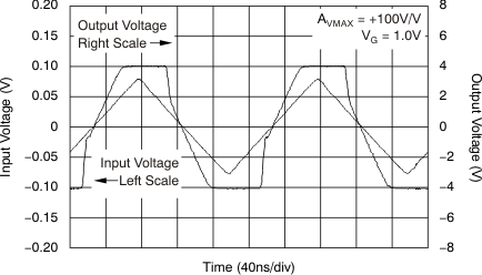 Figure 70. Output Limited Overdrive Recovery
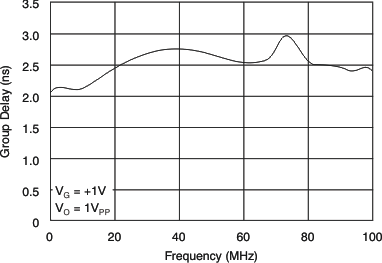 Figure 72. Group Delay vs Frequency