SLUS769D July   2013  – December 2016 UCC28910 , UCC28911

PRODUCTION DATA.  

  1. Features
  2. Applications
  3. Description
  4. Simplified Schematic
  5. Revision History
  6. Device Comparison Table
  7. Pin Configuration and Functions
  8. Detailed Pin Description
    1. 8.1 VDD (Device Voltage Supply)
    2. 8.2 GND (Ground)
    3. 8.3 VS (Voltage Sense)
    4. 8.4 IPK (Set the Maximum DRAIN Current Peak)
    5. 8.5 DRAIN
  9. Specifications
    1. 9.1 Absolute Maximum Ratings
    2. 9.2 Storage Conditions
    3. 9.3 ESD Ratings
    4. 9.4 Recommended Operating Conditions
    5. 9.5 Thermal Information
    6. 9.6 Electrical Characteristics
    7. 9.7 Switching Characteristics
    8. 9.8 Typical Characteristics
  10. 10Detailed Description
    1. 10.1 Overview
    2. 10.2 Functional Block Diagram
    3. 10.3 Feature Description
      1. 10.3.1 Primary-Side Voltage Regulation
      2. 10.3.2 Primary-Side Current Regulation
      3. 10.3.3 Voltage Feed Forward Compensation
      4. 10.3.4 Control Law
      5. 10.3.5 Valley Switching
      6. 10.3.6 Startup Operation
      7. 10.3.7 Fault Protection
        1. 10.3.7.1 Output Over-Voltage
        2. 10.3.7.2 Input Under-Voltage
        3. 10.3.7.3 Primary Over-Current
        4. 10.3.7.4 VDD Clamp Over-Current
        5. 10.3.7.5 Thermal shutdown
      8. 10.3.8 EMI Dithering
    4. 10.4 Device Functional Modes
  11. 11Applications and Implementation
    1. 11.1 Application Information
    2. 11.2 Typical Application
      1. 11.2.1 Battery Charger, 5 V, 6 W
        1. 11.2.1.1 Design Requirements
        2. 11.2.1.2 Detailed Design Procedure
          1. 11.2.1.2.1  Power Handling Curves
          2. 11.2.1.2.2  Input Stage Design and Bulk Capacitance
          3. 11.2.1.2.3  Transformer Turns Ratio
          4. 11.2.1.2.4  Output Capacitance
          5. 11.2.1.2.5  VDD Capacitance, CVDD
          6. 11.2.1.2.6  VS Resistor Divider
          7. 11.2.1.2.7  RVDD Resistor and Turn Ratio
          8. 11.2.1.2.8  Transformer Input Power
          9. 11.2.1.2.9  RIPK Value
          10. 11.2.1.2.10 Transformer Primary Inductance Value
            1. 11.2.1.2.10.1 Secondary Diode Selection
          11. 11.2.1.2.11 Pre-Load
          12. 11.2.1.2.12 DRAIN Voltage Clamp Circuit
      2. 11.2.2 Application Curves
        1. 11.2.2.1 Average Efficiency Performance and Standby Power of the UCC28910FBEVM-526
      3. 11.2.3 Multi-Output Converter with UCC2891x Devices
      4. 11.2.4 Do’s and Don'ts
  12. 12Power Supply Recommendations
  13. 13Layout
    1. 13.1 Layout Guidelines
    2. 13.2 Layout Example
  14. 14Device and Documentation Support
    1. 14.1 Documentation Support
      1. 14.1.1 Device Nomenclature
        1. 14.1.1.1 Definition of Terms
      2. 14.1.2 Related Documents
    2. 14.2 Trademarks
    3. 14.3 Electrostatic Discharge Caution
    4. 14.4 Glossary
    5. 14.5 Related Links
  15. 15Mechanical, Packaging, and Orderable Information

封装选项

机械数据 (封装 | 引脚)
散热焊盘机械数据 (封装 | 引脚)
订购信息

Specifications

Absolute Maximum Ratings

(unless otherwise noted) (1)(2)
MIN MAX UNIT
VDRAIN DRAIN voltage Internally limited(3) 700 V
IDRAIN Negative drain current –100 mA
VDD Supply voltage Internally limited(3) V
IVDD(clp) Maximum VDD clamp current 10 mA
VVS Voltage range Internally limited(3) 7 V
VIPK Voltage range −0.5 5.0 V
IVS Peak VS pin current (current out of the pin) −1.2 mA
IDRAIN Pulsed drain current(4), UCC28910 950 mA
Pulsed drain current(4), UCC28911 1200 mA
TLEAD Lead temperature 1.6 mm (1/16 inch) from case for 10 seconds 260 °C
TJ Operating junction temperature range −55 150 °C
Stresses beyond those listed under Absolute Maximum Ratings may cause permanent damage to the device. These are stress ratings only, which do not imply functional operation of the device at these or any other conditions beyond those indicated under Recommended Operating Conditions. Exposure to absolute-maximum-rated conditions for extended periods may affect device reliability.
All voltages are with respect to GND. Currents are positive into, negative out of the specified pin. These ratings apply over the operating ambient temperature ranges unless otherwise noted.
Do not drive with low impedance voltage source.
Maximum pulse width = 100 μs.

Storage Conditions

MIN MAX UNIT
Tstg Storage temperature −65 150 °C

ESD Ratings

VALUE UNIT
V(ESD) Electrostatic discharge Human-body model (HBM), per ANSI/ESDA/JEDEC JS-001(1) ±2000 V
Charged-device model (CDM), per JEDEC specification JESD22-C101(2) ±500
JEDEC document JEP155 states that 500-V HBM allows safe manufacturing with a standard ESD control process.
JEDEC document JEP157 states that 250-V CDM allows safe manufacturing with a standard ESD control process.

Recommended Operating Conditions(1)(2)

MIN NOM MAX UNIT
VVDD Voltage on VDD terminal during operation VDDOFF VVDD(clp) V
IVS Current out of the terminal 1 mA
ID(peak_max) Maximum drain peak current UCC28910 600 mA
UCC28911 700 mA
TJ Operating junction temperature -40 125 °C
Unless otherwise noted, all voltages are with respect to GND.
In case of thermal shut down, if TA > 100°C, the device does not restart because of the TJ(hys) Electrical Characteristics.

Thermal Information

THERMAL METRIC(1) UCC28910 UCC28911 UNITS
D D
7 Pin SOIC 7 Pin SOIC
θJA Junction-to-ambient thermal resistance 102.2 102.2 °C/W
θJCtop Junction-to-case (top) thermal resistance 39.1 39.1
θJB Junction-to-board thermal resistance 54.7 54.7
ψJT Junction-to-top characterization parameter 5.4 5.4
ψJB Junction-to-board characterization parameter 54.7 54.7
For more information about traditional and new thermal metrics, see the IC Package Thermal Metrics application report, SPRA953.

Electrical Characteristics

over operating free-air temperature range (unless otherwise noted), VVDD = 15 V, TA = -40°C to 125°C, TA = TJ
PARAMETER TEST CONDITIONS MIN TYP MAX UNIT
SUPPLY INPUT
IRUN Supply current, run VVS = 3.9 V, fSW = fSW(max) UCC28910 2.3 2.9 3.4 mA
VVS = 3.75 V, fSW = fSW(max) UCC28911 2.3 2.9 3.4 mA
IRUNQ Quiescent supply current VVS = 3.9 V, fSW = 0 Hz UCC28910 1.90 2.35 2.80 mA
VVS = 3.75 V, fSW = fSW(max) UCC28911 1.90 2.35 2.80 mA
IWAIT Wait supply current VVS = 4.1 V, fSW = fSW(min), TJ = 25°C UCC28910 270 370 µA
UCC28911 250 330 µA
IWAITQ Quiescent wait supply current VVS = 4.1 V, fSW = 0 Hz,
TJ = 25°C
UCC28910 200 280 µA
UCC28911 190 240 µA
ISTART Supply current before start 0 V ≤ VVDD ≤ 5.6 V,
VDRAIN = 0 V
UCC28910 65 90 µA
0 V ≤ VVDD ≤ 5.6 V,
VDRAIN = 0 V, TJ = 25°C
UCC28911 65 80 µA
IFAULT Supply current after fault fSW = 0 Hz UCC28910 190 260 µA
fSW = 0 Hz, TJ = 25°C UCC28911 190 240 µA
UNDER-VOLTAGE LOCKOUT
VDDON VDD turn-on threshold VVDD low to high 9.0 9.5 10.0 V
VDDOFF VDD turn-off threshold VVDD high to low 6.0 6.5 7.0 V
VDDHV(on) HV current source start VVDD high to low 4.8 5.2 5.6 V
ΔVUVLO UVLO hysteresis VDDON – VDDOFF 2.8 3.0 3.2 V
STARTUP CURRENT SOURCE
ICH1 Startup current with VDD shorted to GND VVDD < 250 mV, VDRAIN = 100 V –300 –100 µA
ICH2 Sourced current for startup at high VDD VVDD = 8 V, VDRAIN = 100 V –9.75 –0.40 mA
ICH3 Sourced current for startup at low VDD VVDD = 2 V, VDRAIN = 100 V –13.75 –1.30 mA
VS INPUT
VVSR Regulating level Measured in no load condition,
TJ = 25°C
4.01 4.05 4.09 V
VVSNC Negative clamp level IVS = –300 μA –190 –250 –325 mV
IVS Input bias current VVS = 4 V –0.25 0.00 0.25 µA
PROTECTION
ID(ocp) DRAIN over current IPK pin shorted to GND UCC28910 725 850 925 mA
UCC28911 880 980 1090 mA
VCSTE_OCP Equivalent VCST(OCP),
ID(ocp) x RIPK
VVS = 3.9 V UCC28910 670 770 830 V
VVS = 3.75 V UCC28911 800 885 975 V
VCSTE_OCP2 Equivalent VCST(OCP2)
ID(ocp2) x RIPK
VVS = 3.9 V UCC28910 1200 V
VVS = 3.75 V UCC28911 1400 V
tONMAX(max) Maximum FET on time at high load VVS < 3.9 V, IPK shorted to GND UCC28910 13 18 24 µs
VVS = 3.75 V, IPK shorted to GND UCC28911 13 18 24 µs
tONMAX(min) Maximum FET on time at low load VVS > 4.1 V, IPK shorted to GND UCC28910 4.3 6 10 µs
VVS = 4.35 V, IPK shorted to GND UCC28911 4.3 6 10 µs
VOVP Over-voltage threshold At VS input, TJ = 25°C 4.45 4.60 4.75 V
IVSL(run) VS line sense run current Current out of VS pin – increasing 175 215 260 µA
IVSL(stop) VS line sense stop current Current out of VS pin – decreasing 60 75 100 µA
KVSL Line sense IVS ratio IVSL(run) / IVSL(stop) 2.55 2.70 2.90 A/A
VDDCLP VDD voltage clamp IVDDCLP forced = 2 mA 26 28 30 V
IVDDCLP_OC VDD clamp over current VVDD > 25 V 4.65 6.00 7.65 mA
TJ(stop) Thermal shutdown temperature Internal junction temperature 150 °C
TJ(hys) Thermal shutdown hysteresis Internal junction temperature 50 °C
POWER FET
BVDSS Break-down voltage TJ = 25°C 700 V
RDS(on) Power FET on resistance ID = 150 mA, TJ = 25°C UCC28910 10.5 12.0 Ω
UCC28911 6.25 7.2 Ω
ID = 150 mA, TJ = 125°C UCC28910 18.4 21.5 Ω
UCC28911 11.4 13.4 Ω
ILEAKAGE DRAIN pin leakage current VDS = 400 V HV, VS = 4.2 V DC
TJ = 25°C
10 µA
VDS = 400 V HV, VS = 4.2 V DC
TJ = 125°C
20 µA
VDS = 700 V HV, VS = 4.2 V DC
TJ = 25°C
10 µA
CURRENTS
ID_PEAK(max) Maximum DRAIN peak current IPK pin shorted to GND, TJ = 25°C UCC28910 582 600 618 mA
UCC28911 680 700 720 mA
RIPK_SHORT IPK to GND resistance Max to assume IPK shorted to GND 200 Ω
RIPK(min) IPK to GND minimum resistance 900 Ω
VCSTE(max) Equivalent current sense threshold, ID_PK(max) × RIPK VVS = 3.9 V, TJ = 25°C UCC28910 532 540 548 V
VVS = 3.75 V UCC28911 620 630 640 V
VCSTE(min) Equivalent current sense threshold, ID_PK(min) × RIPK VVS = 4.1 V UCC28910 160 180 200 V
VVS = 4.35 V UCC28911 170 216 265 V
KAM AM control ratio VCSE(max) / VCSE(min) 2.30 3.00 3.50 V/V
KCC CC regulation gain, tDEMAG × fSW VVS < 3.9 V UCC28910 0.413
VVS = 3.75 V UCC28911 0.413
VCCR CC regulation constant,
VCSET(max) × KCC
VVS < 3.9 V, TJ = 25°C UCC28910 216 223 230 V
UCC28911 250 260 270 V

Switching Characteristics

over operating free-air temperature range (unless otherwise noted)
PARAMETER TEST CONDITIONS MIN TYP MAX UNIT
TIMING
fSW(max) Maximum switching frequency VVS < 3.9 V UCC28910 105 115 125 kHz
VVS = 3.75 V UCC28911 105 115 125 kHz
fSW(min) Minimum switching frequency VVS > 4.1 V UCC28910 360 420 490 Hz
VVS = 4.35 V UCC28911 360 420 500 Hz
tZTO Zero crossing timeout delay VVS < 3.9 V UCC28910 1.80 2.10 2.65 µs
VVS = 4.35 V UCC28911 1.80 2.10 2.75 µs
tON(min) Minimum on time IPK = 0.85 V UCC28910 390 ns
UCC28911 420 ns

Typical Characteristics

Unless otherwise specified, VVDD = 15 V, TA = –40°C to 125°C, TA = TJ
UCC28910 UCC28911 C501_SLUS769.png
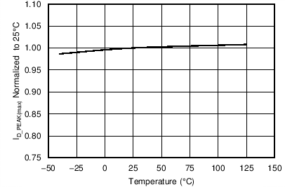
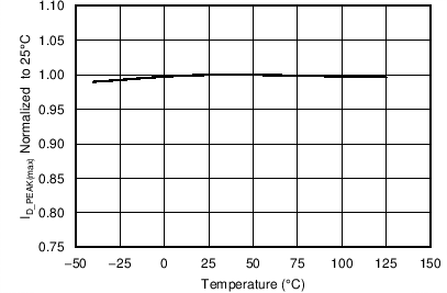
Figure 2. UCC28910 ID_PEAK(max) vs Temperature
UCC28910 UCC28911 C503_SLUS769.png
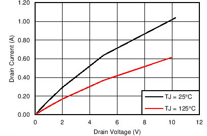
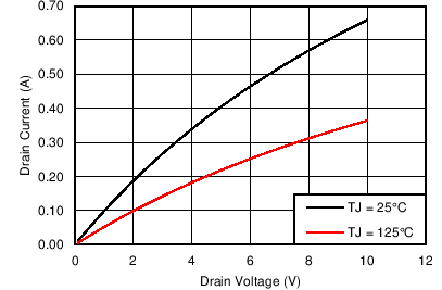
Figure 4. UCC28910 Drain Current vs Drain Voltage
UCC28910 UCC28911 C505_SLUS769.png
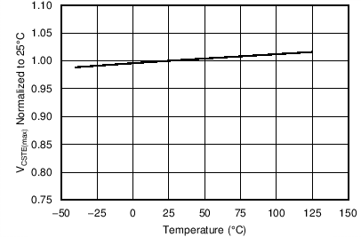
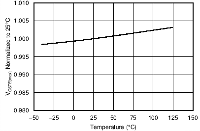
Figure 6. UCC28910 VCSTE(max) vs Temperature
UCC28910 UCC28911 C506_SLUS769.png
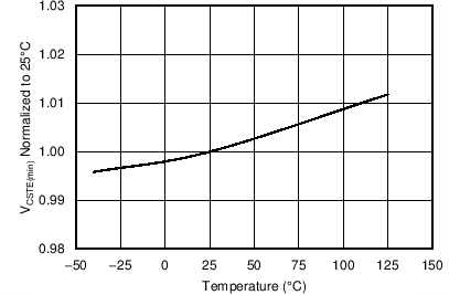
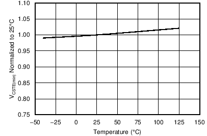
Figure 8. UCC28910 VCSTE(min) vs Temperature
UCC28910 UCC28911 C509_SLUS769.png
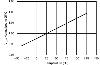
Figure 10. UCC28910 VCCR vs Temperature
UCC28910 UCC28911 C511_SLUS769.png
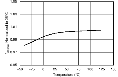
Figure 12. fSW(max) vs Temperature
UCC28910 UCC28911 C513_SLUS769.png
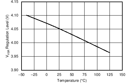
Figure 14. VVSR vs Temperature
UCC28910 UCC28911 C515_SLUS769.png
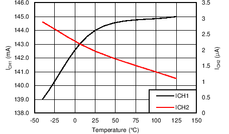
Figure 16. ICH1 and ICH2 vs Temperature
UCC28910 UCC28911 C517_SLUS769.png
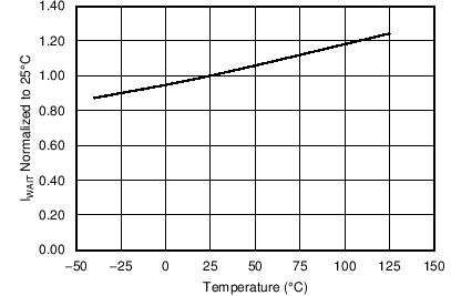
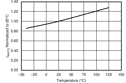
Figure 18. IWAIT vs Temperature
UCC28910 UCC28911 C502_SLUS769.png
Figure 3. UCC28911 ID_PEAK(max) vs Temperature
UCC28910 UCC28911 C504_SLUS769.png
Figure 5. UCC28911 DRAIN Current vs DRAIN Voltage
UCC28910 UCC28911 C507_SLUS769.png
Figure 7. UCC28911 VCSTE(max) vs Temperature
UCC28910 UCC28911 C508_SLUS769.png
Figure 9. UCC28911 VCSTE(min) vs Temperature
UCC28910 UCC28911 C510_SLUS769.png
Figure 11. UCC28911 VCCR vs Temperature
UCC28910 UCC28911 C512_SLUS769.png
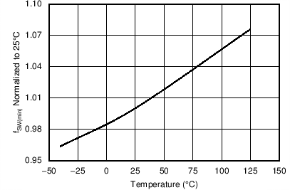
Figure 13. fSW(min) vs Temperature
UCC28910 UCC28911 C514_SLUS769.png
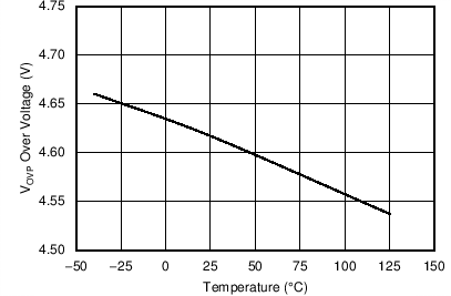
Figure 15. VOVP vs Temperature
UCC28910 UCC28911 C516_SLUS769.png
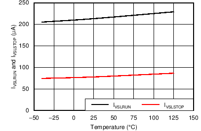
Figure 17. IVSLRUN and IVSLSTOP vs Temperature
UCC28910 UCC28911 C518_SLUS769.png
Figure 19. IWAITQ vs Temperature