SLUS769D July 2013 – December 2016 UCC28910 , UCC28911
PRODUCTION DATA.
- 1 Features
- 2 Applications
- 3 Description
- 4 Simplified Schematic
- 5 Revision History
- 6 Device Comparison Table
- 7 Pin Configuration and Functions
- 8 Detailed Pin Description
- 9 Specifications
-
10Detailed Description
- 10.1 Overview
- 10.2 Functional Block Diagram
- 10.3 Feature Description
- 10.4 Device Functional Modes
-
11Applications and Implementation
- 11.1 Application Information
- 11.2
Typical Application
- 11.2.1
Battery Charger, 5 V, 6 W
- 11.2.1.1 Design Requirements
- 11.2.1.2
Detailed Design Procedure
- 11.2.1.2.1 Power Handling Curves
- 11.2.1.2.2 Input Stage Design and Bulk Capacitance
- 11.2.1.2.3 Transformer Turns Ratio
- 11.2.1.2.4 Output Capacitance
- 11.2.1.2.5 VDD Capacitance, CVDD
- 11.2.1.2.6 VS Resistor Divider
- 11.2.1.2.7 RVDD Resistor and Turn Ratio
- 11.2.1.2.8 Transformer Input Power
- 11.2.1.2.9 RIPK Value
- 11.2.1.2.10 Transformer Primary Inductance Value
- 11.2.1.2.11 Pre-Load
- 11.2.1.2.12 DRAIN Voltage Clamp Circuit
- 11.2.2 Application Curves
- 11.2.3 Multi-Output Converter with UCC2891x Devices
- 11.2.4 Do’s and Don'ts
- 11.2.1
Battery Charger, 5 V, 6 W
- 12Power Supply Recommendations
- 13Layout
- 14Device and Documentation Support
- 15Mechanical, Packaging, and Orderable Information
13 Layout
13.1 Layout Guidelines
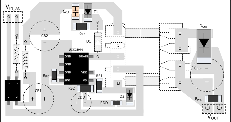
In order to increase the reliability and feasibility of the project it is recommended to follow the here below guidelines.
- Place the RIPK resistance as close as possible to the device with the shortest available traces.
- Try to minimize the area of DRAIN trace, this helps in keeping EMI disturbance low.
- A copper area connected to the GND pins improves heat sinking thermal performance.
- A copper area connected to anode and cathode secondary diode improves heat sinking with an emphasis on the quiet area of the diode, the diode connected to the output capacitor, this limits the EMI disturbance.
- Place the auxiliary voltage sense resistor divider (RS1 and RS2 in Figure 52) directly on the VS pin keeping traces as short as possible.
13.2 Layout Example
 Figure 52. UCC28910 Layout Example