ZHCSHR6A March 2018 – January 2024 UCC27511A
PRODUCTION DATA
- 1
- 1 特性
- 2 应用
- 3 说明
- 4 Pin Configuration and Functions
- 5 Specifications
- 6 Detailed Description
- 7 Application and Implementation
- 8 Power Supply Recommendations
- 9 Layout
- 10Device and Documentation Support
- 11Revision History
- 12Mechanical, Packaging, and Orderable Information
7.2.2.8 Power Dissipation
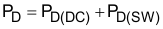
Power dissipation of the gate driver has two portions as shown in Equation 1.
where
- PD is the power dissipation
- PD(DC) is the DC portion of the power dissipation
- PD(SW) is the power dissipated in the gate-driver package during switching
Use Equation 2 to calculate the DC portion of the power dissipation.
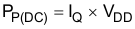
where
- IQ is the quiescent current for the driver
The quiescent current is the current consumed by the device to bias all internal circuits such as input stage, reference voltage, logic circuits, protections, and also any current associated with switching of internal devices when the driver output changes state (such as charging and discharging of parasitic capacitances, parasitic shoot-through, and others). The UCC27511A device features very low quiescent currents (less than 1 mA, see Figure 5-7) and contains internal logic to eliminate any shoot-through in the output driver stage. Thus the effect of the PD(DC) on the total power dissipation within the gate driver can be assumed to be negligible.
The power dissipated in the gate-driver package during switching (PD(SW)) depends on the following factors:
- The gate charge required of the power device (usually a function of the drive voltage VG, which is very close to input bias supply voltage VDD because of low VO(H) drop-out).
- The switching frequency (ƒS)
- Use of external gate resistors (R(GATE))
When a driver device is tested with a discrete, capacitive load calculating the power that is required from the bias supply is fairly simple. The energy to charge the capacitor is given by Equation 3.
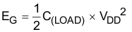
Where
- C(LOAD) is load capacitor
- VDD is bias voltage feeding the driver
- EG is the energy stored in the capacitor when it is charged to VDD
An equal amount of energy dissipates when the capacitor is charged which leads to a total power loss given by Equation 4.
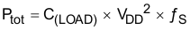
where
- Ptot is the total power loss
- ƒS is the switching frequency
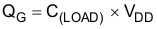
The switching load presented by a power MOSFET or IGBT is converted to an equivalent capacitance by examining the gate charge required to switch the device. This gate charge includes the effects of the input capacitance plus the added charge needed to swing the drain voltage of the power device as it switches between the ON and OFF states. Most manufacturers provide specifications of typical and maximum gate charge, in nC, to switch the device under specified conditions. Using the gate charge, QG, determine the power that must be dissipated when charging a capacitor (calculated using Equation 5, to provide Equation 6).

This power, Ptot, is dissipated in the resistive elements of the circuit when the MOSFET or IGBT is being turned on or off. Half of the total power is dissipated when the load capacitor is charged during turnon, and the other half is dissipated when the load capacitor is discharged during turnoff. When no external gate resistor is employed between the driver and MOSFET or IGBT, this power is completely dissipated inside the driver package. With the use of external gate-drive resistors, the power dissipation is shared between the internal resistance of driver and external gate resistor in accordance to the ratio of the resistance (more power dissipated in the higher resistance component). Based on this simplified analysis, the driver power dissipation during switching is calculated in Equation 7.
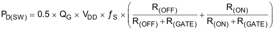
where
- R(OFF) = RO(L)
- R(ON) (effective resistance of pullup structure) = 2.7 × RO(L)