ZHCSJY8E june   2019  – february 2021 UCC256402 , UCC256403 , UCC256404

PRODUCTION DATA  

  1. 特性
  2. 应用
  3. 说明
  4. Revision History
    1.     Device Comparison Table
  5. Pin Configuration and Functions
    1.     Pin Functions
  6. Specifications
    1. 6.1 Absolute Maximum Ratings
    2. 6.2 ESD Ratings
    3. 6.3 Recommended Operating Conditions
    4. 6.4 Thermal Information
    5. 6.5 Electrical Characteristics
    6. 6.6 Switching Characteristics
    7. 6.7 Typical Characteristics
  7. Detailed Description
    1. 7.1 Overview
    2. 7.2 Functional Block Diagram
    3. 7.3 Feature Description
      1. 7.3.1 Hybrid Hysteretic Control
      2. 7.3.2 Regulated 13-V Supply
      3. 7.3.3 Feedback Chain
        1. 7.3.3.1 Optocoupler Feedback Signal Input and Bias
        2. 7.3.3.2 FB Pin Voltage Clamp
        3. 7.3.3.3 "Pick Lower Value" Block and Soft Start Multiplexer
        4. 7.3.3.4 Pick Higher Block and Burst Mode Multiplexer
        5. 7.3.3.5 VCR Comparators
      4. 7.3.4 Resonant Capacitor Voltage Sensing
      5. 7.3.5 Resonant Current Sensing
      6. 7.3.6 Bulk Voltage Sensing
      7. 7.3.7 Output Voltage Sensing
      8. 7.3.8 High Voltage Gate Driver
        1. 7.3.8.1 Adaptive Dead Time Control
      9. 7.3.9 Protections
        1. 7.3.9.1 ZCS Region Prevention
        2. 7.3.9.2 Over Current Protection (OCP)
        3. 7.3.9.3 Bias Winding Over Voltage Protection (BWOVP)
        4. 7.3.9.4 Input Under Voltage Protection (VINUVP)
        5. 7.3.9.5 Input Over Voltage Protection (VINOVP)
        6. 7.3.9.6 Boot UVLO
        7. 7.3.9.7 RVCC UVLO
        8. 7.3.9.8 Over Temperature Protection (OTP)
    4. 7.4 Device Functional Modes
      1. 7.4.1 High Voltage Start-Up
      2. 7.4.2 X-Capacitor Discharge
      3. 7.4.3 Burst Mode Control
        1. 7.4.3.1 Soft-Start and Burst-Mode Threshold
        2. 7.4.3.2 BMTL/BMTH Ratio Programming
      4. 7.4.4 System State Machine
        1.       Application and Implementation
          1. 8.1 Application Information
          2. 8.2 Typical Application
            1. 8.2.1 Design Requirements
            2. 8.2.2 Detailed Design Procedure
              1. 8.2.2.1  LLC Power Stage Requirements
              2. 8.2.2.2  LLC Gain Range
              3. 8.2.2.3  Select Ln and Qe
              4. 8.2.2.4  Determine Equivalent Load Resistance
              5. 8.2.2.5  Determine Component Parameters for LLC Resonant Circuit
              6. 8.2.2.6  LLC Primary-Side Currents
              7. 8.2.2.7  LLC Secondary-Side Currents
              8. 8.2.2.8  LLC Transformer
              9. 8.2.2.9  LLC Resonant Inductor
              10. 8.2.2.10 LLC Resonant Capacitor
              11. 8.2.2.11 LLC Primary-Side MOSFETs
              12. 8.2.2.12 LLC Rectifier Diodes
              13. 8.2.2.13 LLC Output Capacitors
              14. 8.2.2.14 HV Pin Series Resistors
              15. 8.2.2.15 BLK Pin Voltage Divider
              16. 8.2.2.16 ISNS Pin Differentiator
              17. 8.2.2.17 VCR Pin Capacitor Divider
              18. 8.2.2.18 BW Pin Voltage Divider
              19. 8.2.2.19 Soft Start and Burst Mode Programming
            3. 8.2.3 Application Curves
  8. Power Supply Recommendations
    1. 8.1 VCC Pin Capacitor
    2. 8.2 Boot Capacitor
    3. 8.3 RVCC Pin Capacitor
  9. Layout
    1. 9.1 Layout Guidelines
    2. 9.2 Layout Example
  10. 10Device and Documentation Support
    1. 10.1 Documentation Support
      1. 10.1.1 Related Documentation
    2. 10.2 Related Links
    3. 10.3 Receiving Notification of Documentation Updates
    4. 10.4 Community Resources
    5. 10.5 Trademarks
      1.      Mechanical, Packaging, and Orderable Information

封装选项

机械数据 (封装 | 引脚)
散热焊盘机械数据 (封装 | 引脚)
订购信息

LLC Output Capacitors

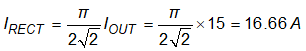
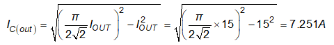
The LLC converter topology does not require an output filter although a small second stage filter inductor may be useful in reducing peak-to-peak output noise. Assuming that the output capacitors carry the rectifier’s full wave output current then the capacitor ripple current rating is:

Equation 40. GUID-733CEC50-E8BC-4342-AEF3-351E185C283A-low.gif

Use 20 V rating for 12-V output voltage:

Equation 41. GUID-041449CE-FE9F-4CCF-9A25-20BC82319193-low.gif

The capacitor’s RMS current rating is:

Equation 42. GUID-BE6DE681-0C3A-4509-9520-9313618FF98D-low.gif

Solid Aluminum capacitors with conductive polymer technology have high ripple-current ratings and are a good choice, especially if the design is required to operate at colder temperatures. The ripple-current rating for a single capacitor may not be sufficient so multiple capacitors are often connected in parallel.

The ripple voltage at the output of the LLC stage is a function of the amount of AC current that flows in the capacitors. To estimate this voltage, assume that all the current, including the DC current in the load, flows in the filter capacitors.

Equation 43. GUID-940193AB-9172-47E0-8786-63EBD6C23E3C-low.gif

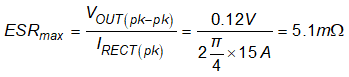
The capacitor specifications are:

  • Voltage Rating: 20 V
  • Ripple Current Rating: 7.251 A
  • ESR: < 5.1 mΩ