ZHCSJY8E june 2019 – february 2021 UCC256402 , UCC256403 , UCC256404
PRODUCTION DATA
- 1 特性
- 2 应用
- 3 说明
- 4 Revision History
- 5 Pin Configuration and Functions
- 6 Specifications
-
7 Detailed Description
- 7.1 Overview
- 7.2 Functional Block Diagram
- 7.3 Feature Description
- 7.4
Device Functional Modes
- 7.4.1 High Voltage Start-Up
- 7.4.2 X-Capacitor Discharge
- 7.4.3 Burst Mode Control
- 7.4.4
System State Machine
-
Application and Implementation
- 8.1 Application Information
- 8.2
Typical Application
- 8.2.1 Design Requirements
- 8.2.2
Detailed Design Procedure
- 8.2.2.1 LLC Power Stage Requirements
- 8.2.2.2 LLC Gain Range
- 8.2.2.3 Select Ln and Qe
- 8.2.2.4 Determine Equivalent Load Resistance
- 8.2.2.5 Determine Component Parameters for LLC Resonant Circuit
- 8.2.2.6 LLC Primary-Side Currents
- 8.2.2.7 LLC Secondary-Side Currents
- 8.2.2.8 LLC Transformer
- 8.2.2.9 LLC Resonant Inductor
- 8.2.2.10 LLC Resonant Capacitor
- 8.2.2.11 LLC Primary-Side MOSFETs
- 8.2.2.12 LLC Rectifier Diodes
- 8.2.2.13 LLC Output Capacitors
- 8.2.2.14 HV Pin Series Resistors
- 8.2.2.15 BLK Pin Voltage Divider
- 8.2.2.16 ISNS Pin Differentiator
- 8.2.2.17 VCR Pin Capacitor Divider
- 8.2.2.18 BW Pin Voltage Divider
- 8.2.2.19 Soft Start and Burst Mode Programming
- 8.2.3 Application Curves
-
Application and Implementation
- 8 Power Supply Recommendations
- 9 Layout
- 10Device and Documentation Support
7.3.1 Hybrid Hysteretic Control
UCC25640x uses a novel control scheme, Hybrid Hysteretic Control (HHC), to achieve best-in-class line and load transient performance. The control method makes the compensator easier to design. The control method also makes light load management easier and more efficient. Improved line transient enables lower bulk capacitor and output capacitor values, reducing system cost.
HHC is a control method which combines traditional frequency control and charge control. It is a charge control with an added frequency compensation ramp. Compared with traditional frequency control, it changes the power stage transfer function from a second order system to a first order system, so that it makes the compensation network design easier. The control effort is directly related to input current, so superior line and load transients can be achieved. Compared with charge control, Hybrid Hysteretic Control avoids instability by adding in a frequency compensation ramp. The frequency compensation ensures system stability, and makes the output impedance lower as well. Lower output impedance makes the transient performance better than charge control. The frequency compensation also makes the implementation of burst mode soft-on and soft-off much easier, as changing the control effort can directly impact the switching frequency. For burst mode soft-on and soft-off, the converter switching frequency self-adjusts to achieve a reduced resonant current.
In summary, HHC solves the following problems:
- Help LLC converters achieve superior load transient and line transient
- Changes the small-signal transfer function to a first order system to easily achieve very high bandwidth
- Inherently stable via frequency compensation
- Makes burst mode control easier to optimize light load efficiency
- Makes the implementation of burst mode soft-on and soft-off much easier, to achieve lower audible noise
Figure 7-1 shows the HHC implementation in UCC25640x: a capacitor divider (C1 and C2) and two well matched controlled current sources. The resonant capacitor voltage is divided down by the capacitor divider formed by C1 and C2. The current sources are controlled by the gate drive signals. When the high-side switch is on, the upper current source injects a constant current into the capacitor divider; when the low-side switch is on, the lower current source pulls the same amount of constant current out of the capacitor divider. The two current sources add a triangular compensation ramp to the VCR node. The current sources are supplied by a reference voltage AVDD. AVDD needs to be equal to or larger than twice the common mode voltage VCM. The divided resonant capacitor voltage and the compensation ramp voltage are then added together to get the VCR node voltage. If the frequency compensation ramp dominates, the VCR node voltage will look like a triangular waveform, and the control will be similar to direct frequency control. If the resonant capacitor voltage dominates, the shape of the VCR node voltage will look like the actual resonant capacitor voltage, and the control will be similar to charge control. This is why the control method is called “hybrid” and the compensation ramp is called frequency compensation.
This set up has an inherent negative feedback to keep the high-side and low-side on-time balanced, and also to keep the common mode voltage at the VCR node at VCM.
There are two input signals needed for the new control scheme: VCR and VCOMP. VCR is the sum of the scaled down version of the resonant capacitor voltage and the frequency compensation ramp. VCOMP is the voltage loop compensator output. The waveform below shows how the high-side and low-side switches are controlled based on VCR and VCOMP. The common mode voltage of VCR is VCM.
Based on VCOMP and VCM (3 V), two thresholds: VTH and VTL are created.
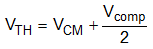
The VCR voltage is compared with the two thresholds. When VCR > VTH, the high-side switch is turned off; when VCR < VTL, low-side switch is turned off. HO and LO turn on edges are controlled by the adaptive dead time circuit.
 Figure 7-1 UCC25640x HHC Implementation
 Figure 7-2 HHC Gate On/Off Control Principle