ZHCSMQ3B august 2020 – may 2023 UCC21710
PRODUCTION DATA
- 1
- 1 特性
- 2 应用
- 3 说明
- 4 Revision History
- 5 Pin Configuration and Functions
-
6 Specifications
- 6.1 Absolute Maximum Ratings
- 6.2 ESD Ratings
- 6.3 Recommended Operating Conditions
- 6.4 Thermal Information
- 6.5 Power Ratings
- 6.6 Insulation Specifications
- 6.7 Safety-Related Certifications
- 6.8 Safety Limiting Values
- 6.9 Electrical Characteristics
- 6.10 Switching Characteristics
- 6.11 Insulation Characteristics Curves
- 6.12 Typical Characteristics
- 7 Parameter Measurement Information
-
8 Detailed Description
- 8.1 Overview
- 8.2 Functional Block Diagram
- 8.3
Feature Description
- 8.3.1 Power Supply
- 8.3.2 Driver Stage
- 8.3.3 VCC and VDD Undervoltage Lockout (UVLO)
- 8.3.4 Active Pulldown
- 8.3.5 Short Circuit Clamping
- 8.3.6 Internal Active Miller Clamp
- 8.3.7 Overcurrent and Short Circuit Protection
- 8.3.8 Soft Turn-off
- 8.3.9 Fault ( FLT, Reset and Enable ( RST/EN)
- 8.3.10 Isolated Analog to PWM Signal Function
- 8.4 Device Functional Modes
-
9 Applications and Implementation
- 9.1 Application Information
- 9.2
Typical Application
- 9.2.1 Design Requirements
- 9.2.2
Detailed Design Procedure
- 9.2.2.1 Input filters for IN+, IN- and RST/EN
- 9.2.2.2 PWM Interlock of IN+ and IN-
- 9.2.2.3 FLT, RDY and RST/EN Pin Circuitry
- 9.2.2.4 RST/EN Pin Control
- 9.2.2.5 Turn on and turn off gate resistors
- 9.2.2.6 Overcurrent and Short Circuit Protection
- 9.2.2.7 Isolated Analog Signal Sensing
- 9.2.2.8 Higher Output Current Using an External Current Buffer
- 10Power Supply Recommendations
- 11Layout
- 12Device and Documentation Support
- 13Mechanical, Packaging, and Orderable Information
9.2.2.6.3 Protection Based on Shunt Resistor in Power Loop
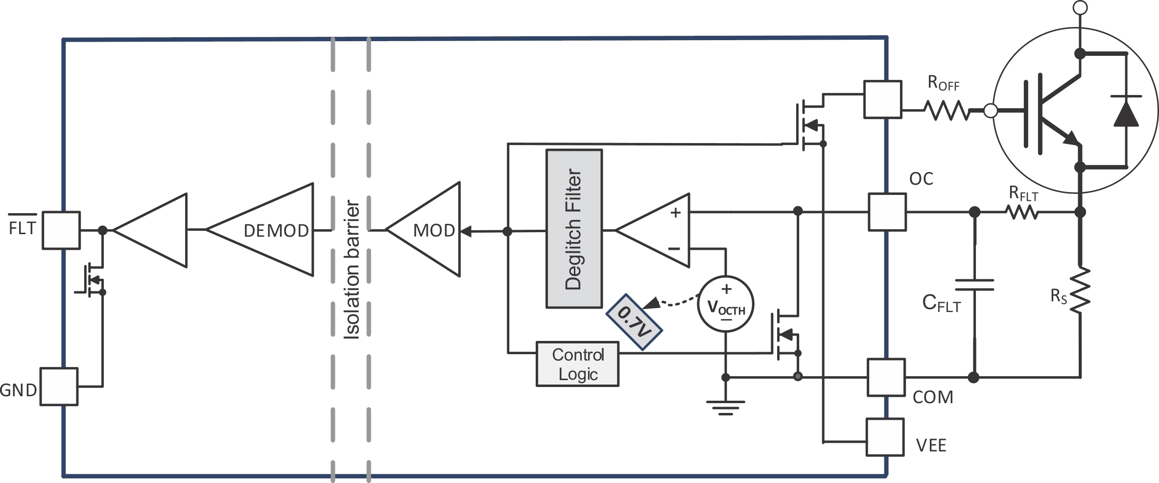
In lower power applications, to simplify the circuit and reduce the cost, a shunt resistor can be used in series in the power loop and measure the current directly. Since the resistor is in series in the power loop, it directly measures the current and can have high accuracy by using a high precision resistor. The resistance needs to be small to reduce the power loss, and should have large enough voltage resolution for the protection. Since the sensing resistor is also in series in the gate driver loop, the voltage drop on the sensing resistor can cause the voltage drop on the gate voltage of the IGBT or SiC MOSFET modules. The parasitic inductance of the sensing resistor and the PCB trace of the sensing loop will also cause a noise voltage source during switching transient, which makes the gate voltage oscillate. Thus, this method is not recommended for high power application, or when dI/dt is high. To use it in low power application, the shunt resistor loop should be designed to have the optimal voltage drop and minimum noise injection to the gate loop.
 Figure 9-9 Overcurrent and Short Circuit Protection Based on Shunt Resistor