ZHCSQX4F August   1995  – August 2022 UC1823A , UC1825A , UC2823A , UC2823B , UC2825A , UC2825B , UC3823A , UC3823B , UC3825A , UC3825B

PRODUCTION DATA  

  1. 1特性
  2. 2说明
  3. 3Revision History
  4. 4Ordering Information
  5. 5Pin Configuration and Functions
    1.     Terminal Functions
  6. 6Specifications
    1. 6.1 ABSOLUTE MAXIMUM RATINGS
    2. 6.2 Thermal Information
    3. 6.3 ELECTRICAL CHARACTERISTICS
    4. 6.4 ELECTRICAL CHARACTERISTICS
  7. 7Application and Implementation
    1. 7.1 LEADING EDGE BLANKING
    2. 7.2 UVLO、软启动和故障管理
    3. 7.3 ACTIVE LOW OUTPUTS DURING UVLO
    4. 7.4 CONTROL METHODS
    5. 7.5 SYNCHRONIZATION
    6. 7.6 HIGH CURRENT OUTPUTS
    7. 7.7 GROUND PLANES
    8. 7.8 OPEN LOOP TEST CIRCUIT
  8. 8Device and Documentation Support
    1. 8.1 Documentation Support
    2. 8.2 接收文档更新通知
    3. 8.3 支持资源
    4. 8.4 Trademarks
    5. 8.5 Electrostatic Discharge Caution
    6. 8.6 术语表
  9. 9Mechanical, Packaging, and Orderable Information

封装选项

请参考 PDF 数据表获取器件具体的封装图。

机械数据 (封装 | 引脚)
  • DW|16
散热焊盘机械数据 (封装 | 引脚)
订购信息

ACTIVE LOW OUTPUTS DURING UVLO

The UVLO function forces the outputs to be low and considers both VCC and VREF before allowing the chip to operate.
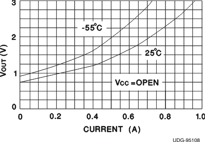
GUID-FEC3E750-1A85-4D26-8C44-A06DDB2CDACF-low.gifFigure 7-3 Output Voltage vs Output Current
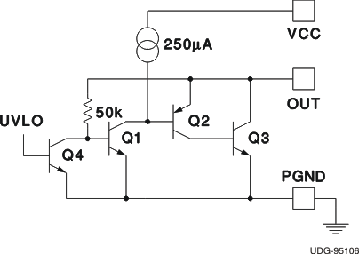
GUID-8B3F219E-8C2B-43F2-A9ED-C003C9B4BEF0-low.gifFigure 7-4 Output V and I During UVLO