SLUS191D February 1997 – July 2017 UC1525A , UC1527A , UC2525A , UC2527A , UC3525A , UC3527A
PRODUCTION DATA.
- 1 Features
- 2 Applications
- 3 Description
- 4 Revision History
- 5 Pin Configuration and Functions
- 6 Specifications
- 7 Detailed Description
- 8 Application and Implementation
- 9 Power Supply Recommendations
- 10Layout
- 11Device and Documentation Support
- 12Mechanical, Packaging, and Orderable Information
7 Detailed Description
7.1 Overview
The UCx52xA series of pulse width modulator integrated circuits are designed to offer improved performance and lowered external parts count when used in designing all types of switching power supplies. The on-chip
5.1-V reference is trimmed to 1% and the input common-mode range of the error amplifier includes the reference voltage, eliminating external resistors. A sync input to the oscillator allows multiple units to be slaved or a single unit to be synchronized to an external system clock. A single resistor between CT and the discharge terminals provides a wide range of dead-time adjustment. These devices also feature built-in soft-start circuitry with only an external timing capacitor required. A shutdown terminal controls both the soft-start circuitry and the output stages, providing instantaneous turn off through the PWM latch with pulsed shutdown, as well as soft-start recycle with longer shutdown commands.
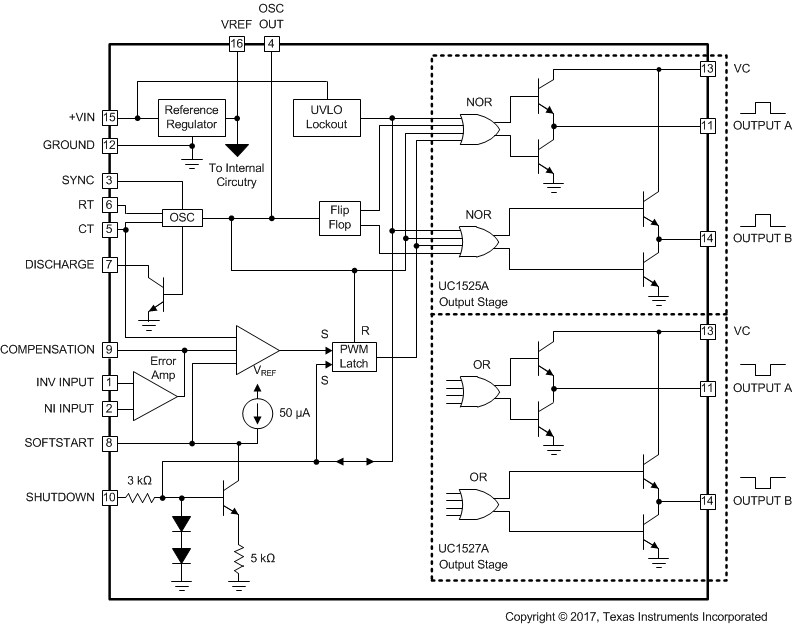
These functions are also controlled by an undervoltage lockout which keeps the outputs off and the soft-start capacitor discharged for subnormal input voltages. This lockout circuitry includes approximately 500 mV of hysteresis for jitter-free operation. Another feature of these PWM circuits is a latch following the comparator. Once a PWM pulse has been terminated for any reason, the outputs will remain off for the duration of the period. The latch is reset with each clock pulse. The output stages are totem-pole designs capable of sourcing or sinking in excess of 200 mA. The UC1525A output stage features NOR logic, giving a LOW output for an OFF state. The UC1527A uses OR logic, which results in a HIGH output level when OFF.
7.2 Functional Block Diagram

7.3 Feature Description
7.3.1 Adjustable Dead-Time Control
A single resistor between CT and the discharge terminals provides a wide range of dead-time adjustment.
7.3.2 Soft Start
Soft start is achieved by connecting the soft-start pin to ground through a capacitor, charged by the 50-µA current source. See Functional Block Diagram.
7.3.3 Input Undervoltage Lockout With Hysteresis
The undervoltage lockout keeps the outputs off and the soft-start capacitor discharged for subnormal input voltages. This lockout circuitry includes approximately 500 mV of hysteresis for jitter-free operation.
7.3.4 Shutdown and Pulse-by-Pulse Current Limiting
7.4 Device Functional Modes
This device has no functional modes.
7.4.1 Shutdown Options (See Functional Block Diagram)
Since both the compensation and soft-start terminals have current source pullups, either can readily accept a pull-down signal which only has to sink a maximum of 100 A to turn off the outputs. This is subject to the added requirement of discharging whatever external capacitance may be attached to these pins.
An alternate approach is the use of the shutdown circuitry of the shutdown pin which has been improved to enhance the available shutdown options. Activating this circuit by applying a positive signal on the shutdown pin performs two functions; the PWM latch is immediately set providing the fastest turn-off signal to the outputs; and a 150-A current sink begins to discharge the external soft-start capacitor. If the shutdown command is short, the PWM signal is terminated without significant discharge of the soft-start capacitor, thus, allowing, for example, a convenient implementation of pulse-by-pulse current limiting. Holding the shutdown pin high for a longer duration, however, will ultimately discharge this external capacitor, recycling slow turnon upon release.
The shutdown pin should not be left floating as noise pickup could conceivably interrupt normal operation. All transitions of the voltage on the shutdown pin should be within the time frame of one clock cycle and not repeated at a frequency higher than 10 clock cycles.