ZHCSCV8A September 2014 – October 2014 TUSB1210-Q1
PRODUCTION DATA.
- 1 特性
- 2 应用范围
- 3 说明
- 4 修订历史记录
- 5 Pin Configuration and Functions
-
6 Specifications
- 6.1 Absolute Maximum Ratings
- 6.2 Handling Ratings
- 6.3 Recommended Operating Conditions
- 6.4 Thermal Information
- 6.5 Analog I/O Electrical Characteristics
- 6.6 Digital I/O Electrical Characteristics
- 6.7 Digital IO Pins (Non-ULPI)
- 6.8 PHY Electrical Characteristics
- 6.9 Pullup/Pulldown Resistors
- 6.10 OTG Electrical Characteristics
- 6.11 Power Characteristics
- 6.12 Switching Characteristics
- 6.13 Timing Requirements
- 6.14 Typical Characteristics
-
7 Detailed Description
- 7.1 Overview
- 7.2 Functional Block Diagram
- 7.3 Feature Description
- 7.4 Device Functional Modes
- 7.5
Register Map
- 7.5.1 VENDOR_ID_LO
- 7.5.2 VENDOR_ID_HI
- 7.5.3 PRODUCT_ID_LO
- 7.5.4 PRODUCT_ID_HI
- 7.5.5 FUNC_CTRL
- 7.5.6 FUNC_CTRL_SET
- 7.5.7 FUNC_CTRL_CLR
- 7.5.8 IFC_CTRL
- 7.5.9 IFC_CTRL_SET
- 7.5.10 IFC_CTRL_CLR
- 7.5.11 OTG_CTRL
- 7.5.12 OTG_CTRL_SET
- 7.5.13 OTG_CTRL_CLR
- 7.5.14 USB_INT_EN_RISE
- 7.5.15 USB_INT_EN_RISE_SET
- 7.5.16 USB_INT_EN_RISE_CLR
- 7.5.17 USB_INT_EN_FALL
- 7.5.18 USB_INT_EN_FALL_SET
- 7.5.19 USB_INT_EN_FALL_CLR
- 7.5.20 USB_INT_STS
- 7.5.21 USB_INT_LATCH
- 7.5.22 DEBUG
- 7.5.23 SCRATCH_REG
- 7.5.24 SCRATCH_REG_SET
- 7.5.25 SCRATCH_REG_CLR
- 7.5.26 VENDOR_SPECIFIC1
- 7.5.27 VENDOR_SPECIFIC1_SET
- 7.5.28 VENDOR_SPECIFIC1_CLR
- 7.5.29 VENDOR_SPECIFIC2
- 7.5.30 VENDOR_SPECIFIC2_SET
- 7.5.31 VENDOR_SPECIFIC2_CLR
- 7.5.32 VENDOR_SPECIFIC1_STS
- 7.5.33 VENDOR_SPECIFIC1_LATCH
- 7.5.34 VENDOR_SPECIFIC3
- 7.5.35 VENDOR_SPECIFIC3_SET
- 7.5.36 VENDOR_SPECIFIC3_CLR
- 8 Application and Implementation
- 9 Power Supply Recommendations
- 10Layout
- 11器件和文档支持
- 12机械封装和可订购信息
7 Detailed Description
7.1 Overview
The TUSB1210-Q1 is a USB2.0 transceiver chip, designed to interface with a USB controller via a ULPI interface. It supports all USB2.0 data rates High-Speed, Full-Speed, and Low-Speed. Compliant to both Host and Peripheral (OTG) modes. It additionally supports a UART mode and legacy ULPI serial modes. TUSB1210-Q1 Integrates a 3.3-V LDO, which makes it flexible to work with either battery operated systems or pure 3.3 V supplied systems. Also, it has an integrated PLL Supporting 2 Clock Frequencies 19.2 MHz/26 MHz. The ULPI clock pin (60 MHz) supports both input and output clock configurations. TUSB1210-Q1 has low power consumption, optimized for portable devices, and complete USB OTG Physical Front-End that supports Host Negotiation Protocol (HNP) and Session Request Protocol (SRP).
TUSB1210-Q1 is optimized to be interfaced through a 12-pin SDR UTMI Low Pin Interface (ULPI), supporting both input clock and output clock modes, with 1.8 V interface supply voltage.
TUSB1210-Q1 integrates a 3.3 V LDO, which makes it flexible to work with either battery operated systems or pure 3.3 V supplied systems. Both the main supply and the 3.3 V power domain can be supplied through an external switched-mode converter for optimized power efficiency.
TUSB1210-Q1 includes a POR circuit to detect supply presence on VBAT and VDDIO pins. TUSB1210-Q1 can be disabled or configured in low power mode for energy saving.
TUSB1210-Q1 is protected against accidental shorts to 5 V or ground on its exposed interface (DP/DM/ID). It is also protected against up to 20 V surges on VBUS.
TUSB1210-Q1 integrates a high-performance low-jitter 480 MHz PLL and supports two clock configurations. Depending on the required link configuration, TUSB1210-Q1 supports both ULPI input and output clock mode : input clock mode, in which case a square-wave 60 MHz clock is provided to TUSB1210-Q1 at the ULPI interface CLOCK pin; and output clock mode in which case TUSB1210-Q1 can accept a square-wave reference clock at REFCLK of either 19.2 MHz, 26 MHz. Frequency is indicated to TUSB1210-Q1 via the configuration pin CFG. This can be useful if a reference clock is already available in the system.
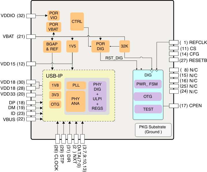
7.2 Functional Block Diagram
7.3 Feature Description
7.3.1 Processor Subsystem
7.3.1.1 Clock Specifications
7.3.1.1.1 USB PLL Reference Clock
The USB PLL block generates the clocks used to synchronize :
- the ULPI interface (60 MHz clock)
- the USB interface (depending on the USB data rate, 480 Mbps, 12 Mbps or 1.5 Mbps)
TUSB1210-Q1 requires an external reference clock which is used as an input to the 480 MHz USB PLL block. Depending on the clock configuration, this reference clock can be provided either at REFCLK pin or at CLOCK pin. By default CLK pin is configured as an input.
Two clock configurations are possible:
- Input clock configuration (see ULPI Input Clock Configuration)
- Output clock configuration (see ULPI Output Clock Configuration)
7.3.1.1.2 ULPI Input Clock Configuration
In this mode REFCLK must be externally tied to GND. CLOCK remains configured as an input.
When the ULPI interface is used in input clock configuration, that is, the 60 MHz ULPI clock is provided to TUSB1210-Q1 on Clock pin, then this is used as the reference clock for the 480 MHz USB PLL block. See Switching Characteristics.
7.3.1.1.3 ULPI Output Clock Configuration
In this mode a reference clock must be externally provided on REFCLK pin When an input clock is detected on REFCLK pin then CLK will automatically change to an output, i.e., 60 MHz ULPI clock is output by TUSB1210-Q1 on CLK pin.
Two reference clock input frequencies are supported. REFCLK input frequency is communicated to TUSB1210-Q1 via a configuration pin, CFG, see fREFCLK in Table 11 for frequency correspondence. TUSB1210-Q1 supports square-wave reference clock input only. Reference clock input must be square-wave of amplitude in the range 3 V to 3.6 V. See Switching Characteristics.
7.3.1.1.4 Clock 32 kHz
An internal clock generator running at 32 kHz has been implemented to provide a low-speed, low-power clock to the system See Clock 32 kHz
7.3.1.1.5 Reset
All logic is reset if CS = 0 or VBAT are not present.
All logic (except 32 kHz logic) is reset if VDDIO is not present.
PHY logic is reset when any supplies are not present (VDDIO, VDD15, VDD18, VDD33) or if RESETB pin is low.
TUSB1210-Q1 may be reset manually by toggling the RESETB pin to GND for at lease 200 ns.
If manual reset via RESETB is not required then RESETB pin may be tied to VDDIO permanently.
7.3.1.2 USB Transceiver
The TUSB1210-Q1 device includes a universal serial bus (USB) on-the-go (OTG) transceiver that supports USB 480 Mb/s high-speed (HS), 12 Mb/s full-speed (FS), and USB 1.5 Mb/s low-speed (LS) through a 12-pin UTMI+ low pin interface (ULPI).
NOTE
LS device mode is not allowed by a USB2.0 HS capable PHY, therefore it is not supported by TUSB1210-Q1. This is stated in USB2.0 standard Chapter 7, page 119, second paragraph: “A high-speed capable upstream facing transceiver must not support low-speed signaling mode..” There is also some related commentary in Chapter 7.1.2.3.
7.3.1.2.1 PHY Electrical Characteristics
The PHY is the physical signaling layer of the USB 2.0. It essentially contains all the drivers and receivers required for physical data and protocol signaling on the DP and DM lines.
The PHY interfaces to the USB controller through a standard 12-pin digital interface called UTMI+ low pin interface (ULPI).
The transmitters and receivers inside the PHY are classified into two main classes.
- The full-speed (FS) and low-speed (LS) transceivers. These are the legacy USB1.x transceivers.
- The HS (HS) transceivers
In order to bias the transistors and run the logic, the PHY also contains reference generation circuitry which consists of:
- A DPLL which does a frequency multiplication to achieve the 480-MHz low-jitter lock necessary for USB and also the clock required for the switched capacitor resistance block.
- A switched capacitor resistance block which is used to replicate an external resistor on chip.
Built-in pullup and pulldown resistors are used as part of the protocol signaling.
Apart from this, the PHY also contains circuitry which protects it from accidental 5-V short on the DP and DM lines.
7.3.1.2.1.1 LS/FS Single-Ended Receivers
In addition to the differential receiver, there is a single-ended receiver (SE–, SE+) for each of the two data lines D+/–. The main purpose of the single-ended receivers is to qualify the D+ and D– signals in the full-speed/low-speed modes of operation. See PHY Electrical Characteristics.
7.3.1.2.1.2 LS/FS Differential Receiver
A differential input receiver (Rx) retrieves the LS/FS differential data signaling. The differential voltage on the line is converted into digital data by a differential comparator on DP/DM. This data is then sent to a clock and data recovery circuit which recovers the clock from the data. An additional serial mode exists in which the differential data is directly output on the RXRCV pin. See Switching Characteristics.
7.3.1.2.1.3 LS/FS Transmitter
The USB transceiver (Tx) uses a differential output driver to drive the USB data signal D+/– onto the USB cable. The driver's outputs support 3-state operation to achieve bidirectional half-duplex transactions. See Switching Characteristics.
7.3.1.2.1.4 HS Differential Receiver
The HS receiver consists of the following blocks:
A differential input comparator to receive the serial data
- A squelch detector to qualify the received data
- An oversampler-based clock data recovery scheme followed by a NRZI decoder, bit unstuffing, and serial-to-parallel converter to generate the ULPI DATAOUT
7.3.1.2.1.5 HS Differential Transmitter
The HS transmitter is always operated via the ULPI parallel interface. The parallel data on the interface is serialized, bit stuffed, NRZI encoded, and transmitted as a dc output current on DP or DM depending on the data. Each line has an effective 22.5-Ω load to ground, which generates the voltage levels for signaling.
A disconnect detector is also part of the HS transmitter. A disconnect on the far end of the cable causes the impedance seen by the transmitter to double thereby doubling the differential amplitude seen on the DP/DM lines of Switching Characteristics.
7.3.1.2.1.6 UART Transceiver
In this mode, the ULPI data bus is redefined as a 2-pin UART interface, which exchanges data through a direct access to the FS/LS analog transmitter and receiver. See Switching Characteristics.
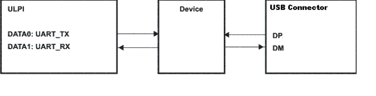 Figure 4. USB UART Data Flow
7.3.1.2.2 OTG Characteristics
The on-the-go (OTG) block integrates three main functions:
- The USB plug detection function on VBUS and ID
- The ID resistor detection
- The VBUS level detection
7.4 Device Functional Modes
7.4.1 TUSB1210-Q1 Modes vs ULPI Pin Status
Table 5, Table 6, and Table 7 show the status of each of the 12 ULPI pins including input/output direction and whether output pins are driven to ‘0’ or to ‘1’, or pulled up/pulled down via internal pullup/pulldown resistors.
Note that pullup/pulldown resistors are automatically replaced by driven ‘1’/’0’ levels respectively once internal IORST is released, with the exception of the pullup on STP which is maintained in all modes.
Pin assignment changes in ULPI 3-pin serial mode, ULPI 6-pin serial mode, and UART mode. Unused pins are tied low in these modes as shown below.
Table 5. TUSB1210-Q1 Modes vs ULPI Pin Status:ULPI Synchronous Mode Power-Up
| ULPI SYNCHRONOUS MODE POWER-UP | |||||||||
|---|---|---|---|---|---|---|---|---|---|
| UNTIL IORST RELEASE | PLL OFF | PLL ON + STP HIGH | PLL ON + STP LOW | ||||||
| PIN NO. | PIN NAME | DIR | PU/PD | DIR | PU/PD | DIR | PU/PD | DIR | PU/PD |
| 26 | CLOCK | Hiz | PD | I | PD | IO | - | IO | - |
| 31 | DIR | Hiz | PU | O, (‘1’) | - | O, (‘0’) | - | O | - |
| 2 | NXT | Hiz | PD | O, (‘0’) | - | O, (‘0’) | - | O | - |
| 29 | STP | Hiz | PU | I | PU | I | PU | I | PU |
| 3 | DATA0 | Hiz | PD | O, (‘0’) | - | I | PD | IO | - |
| 4 | DATA1 | Hiz | PD | O, (‘0’) | - | I | PD | IO | - |
| 5 | DATA2 | Hiz | PD | O, (‘0’) | - | I | PD | IO | - |
| 6 | DATA3 | Hiz | PD | O, (‘0’) | - | I | PD | IO | - |
| 7 | DATA4 | Hiz | PD | O, (‘0’) | - | I | PD | IO | - |
| 9 | DATA5 | Hiz | PD | O, (‘0’) | - | I | PD | IO | - |
| 10 | DATA6 | Hiz | PD | O, (‘0’) | - | I | PD | IO | - |
| 13 | DATA7 | Hiz | PD | O, (‘0’) | - | I | PD | IO | - |
Table 6. TUSB1210-Q1 Modes vs ULPI Pin Status: USB Suspend Mode
| SUSPEND MODE | LINK / EXTERNAL RECOMMENDED SETTING DURING SUSPEND MODE | ||||
|---|---|---|---|---|---|
| PIN NO. | PIN NAME | DIR | PU/PD | DIR | PU/PD |
| 26 | CLOCK | I | - | O | - |
| 31 | DIR | O, (‘1’) | - | I | - |
| 2 | NXT | O, (‘0’) | - | I | - |
| 29 | STP | I | PU(1) | O, (‘0’) | - |
| 3 | DATA0 | O, (LINESTATE0) | - | I | - |
| 4 | DATA1 | O, (LINESTATE1) | - | I | - |
| 5 | DATA2 | O, (‘0’) | - | I | - |
| 6 | DATA3 | O, (INT) | - | I | - |
| 7 | DATA4 | O, (‘0’) | - | I | - |
| 9 | DATA5 | O, (‘0’) | - | I | - |
| 10 | DATA6 | O, (‘0’) | - | I | - |
| 13 | DATA7 | O, (‘0’) | - | I | - |
Table 7. TUSB1210-Q1 Modes vs ULPI Pin Status: ULPI 6-Pin Serial Mode and UART Mode
| ULPI 6-PIN SERIAL MODE | ULPI 3-PIN SERIAL MODE | UART MODE | |||||||
|---|---|---|---|---|---|---|---|---|---|
| PIN NO. | PIN NAME | DIR | PU/PD | PIN NAME | DIR | PU/PD | PIN NAME | DIR | PU/PD |
| 26 | CLOCK (1) | IO | - | CLOCK (1) | IO | - | CLOCK (1) | IO | - |
| 31 | DIR | O | - | DIR | O | - | DIR | O | - |
| 2 | NXT | O | - | NXT | O | - | NXT | O | - |
| 29 | STP | I | PU | STP | I | PU | STP | I | PU |
| 3 | TX_ENABLE | I | - | TX_ENABLE | I | - | TXD | I | - |
| 4 | TX_DAT | I | - | DAT | IO | - | RXD | IO | - |
| 5 | TX_SE0 | I | - | SE0 | IO | - | tie low | O | - |
| 6 | INT | O | - | INT | O | - | INT | O | - |
| 7 | RX_DP | O | - | tie low | O | - | tie low | O | - |
| 9 | RX_DM | O | - | tie low | O | - | tie low | O | - |
| 10 | RX_RCV | O | - | tie low | O | - | tie low | O | - |
| 13 | tie low | O | - | tie low | O | - | tie low | O | - |
7.5 Register Map
Table 8. USB Register Summary
| REGISTER NAME | TYPE | REGISTER WIDTH (BITS) | PHYSICAL ADDRESS |
|---|---|---|---|
| VENDOR_ID_LO | R | 8 | 0x00 |
| VENDOR_ID_HI | R | 8 | 0x01 |
| PRODUCT_ID_LO | R | 8 | 0x02 |
| PRODUCT_ID_HI | R | 8 | 0x03 |
| FUNC_CTRL | RW | 8 | 0x04 |
| FUNC_CTRL_SET | RW | 8 | 0x05 |
| FUNC_CTRL_CLR | RW | 8 | 0x06 |
| IFC_CTRL | RW | 8 | 0x07 |
| IFC_CTRL_SET | RW | 8 | 0x08 |
| IFC_CTRL_CLR | RW | 8 | 0x09 |
| OTG_CTRL | RW | 8 | 0x0A |
| OTG_CTRL_SET | RW | 8 | 0x0B |
| OTG_CTRL_CLR | RW | 8 | 0x0C |
| USB_INT_EN_RISE | RW | 8 | 0x0D |
| USB_INT_EN_RISE_SET | RW | 8 | 0x0E |
| USB_INT_EN_RISE_CLR | RW | 8 | 0x0F |
| USB_INT_EN_FALL | RW | 8 | 0x10 |
| USB_INT_EN_FALL_SET | RW | 8 | 0x11 |
| USB_INT_EN_FALL_CLR | RW | 8 | 0x12 |
| USB_INT_STS | R | 8 | 0x13 |
| USB_INT_LATCH | R | 8 | 0x14 |
| DEBUG | R | 8 | 0x15 |
| SCRATCH_REG | RW | 8 | 0x16 |
| SCRATCH_REG_SET | RW | 8 | 0x17 |
| SCRATCH_REG_CLR | RW | 8 | 0x18 |
| Reserved | R | 8 | 0x19 0x2E |
| ACCESS_EXT_REG_SET | RW | 8 | 0x2F |
| Reserved | R | 8 | 0x30 0x3C |
| VENDOR_SPECIFIC1 | RW | 8 | 0x3D |
| VENDOR_SPECIFIC1_SET | RW | 8 | 0x3E |
| VENDOR_SPECIFIC1_CLR | RW | 8 | 0x3F |
| VENDOR_SPECIFIC2 | RW | 8 | 0x80 |
| VENDOR_SPECIFIC2_SET | RW | 8 | 0x81 |
| VENDOR_SPECIFIC2_CLR | RW | 8 | 0x82 |
| VENDOR_SPECIFIC1_STS | R | 8 | 0x83 |
| VENDOR_SPECIFIC1_LATCH | R | 8 | 0x84 |
| VENDOR_SPECIFIC3 | RW | 8 | 0x85 |
| VENDOR_SPECIFIC3_SET | RW | 8 | 0x86 |
| VENDOR_SPECIFIC3_CLR | RW | 8 | 0x87 |
7.5.1 VENDOR_ID_LO
| ADDRESS OFFSET | 0x00 | ||
| PHYSICAL ADDRESS | 0x00 | INSTANCE | USB_SCUSB |
| DESCRIPTION | Lower byte of vendor ID supplied by USB-IF (TI Vendor ID = 0x0451) | ||
| TYPE | R | ||
| WRITE LATENCY | |||
| 7 | 6 | 5 | 4 | 3 | 2 | 1 | 0 |
| VENDOR_ID | |||||||
| BITS | FIELD NAME | DESCRIPTION | TYPE | RESET |
| 7:00 | VENDOR_ID | R | 0x51 |
7.5.2 VENDOR_ID_HI
| ADDRESS OFFSET | 0x01 | ||
| PHYSICAL ADDRESS | 0x01 | INSTANCE | USB_SCUSB |
| DESCRIPTION | Upper byte of vendor ID supplied by USB-IF (TI Vendor ID = 0x0451) | ||
| TYPE | R | ||
| WRITE LATENCY | |||
| 7 | 6 | 5 | 4 | 3 | 2 | 1 | 0 |
| VENDOR_ID | |||||||
| BITS | FIELD NAME | DESCRIPTION | TYPE | RESET |
| 7:00 | VEN DOR_ID | R | 0x04 |
7.5.3 PRODUCT_ID_LO
| ADDRESS OFFSET | 0x02 | ||
| PHYSICAL ADDRESS | 0x02 | INSTANCE | USB_SCUSB |
| DESCRIPTION | Lower byte of Product ID supplied by Vendor (TUSB1210-Q1 Product ID is 0x1507). | ||
| TYPE | R | ||
| WRITE LATENCY | |||
| 7 | 6 | 5 | 4 | 3 | 2 | 1 | 0 |
| PRODUCT_ID | |||||||
| BITS | FIELD NAME | DESCRIPTION | TYPE | RESET |
| 7:00 | PRODUCT_ID | R | 0x07 | |
7.5.4 PRODUCT_ID_HI
| ADDRESS OFFSET | 0x03 | ||
| PHYSICAL ADDRESS | 0x03 | INSTANCE | USB_SCUSB |
| DESCRIPTION | Upper byte of Product ID supplied by Vendor (TUSB1210-Q1 Product ID is 0x1507). | ||
| TYPE | R | ||
| WRITE LATENCY | |||
| 7 | 6 | 5 | 4 | 3 | 2 | 1 | 0 |
| PRODUCT_ID | |||||||
| BITS | FIELD NAME | DESCRIPTION | TYPE | RESET |
| 7:00 | PRODUCT_ID | R | 0x15 | |
7.5.5 FUNC_CTRL
| ADDRESS OFFSET | 0x04 | ||
| PHYSICAL ADDRESS | 0x04 | INSTANCE | USB_SCUSB |
| DESCRIPTION | Controls UTMI function settings of the PHY. | ||
| TYPE | RW | ||
| WRITE LATENCY | |||
| 7 | 6 | 5 | 4 | 3 | 2 | 1 | 0 |
|---|---|---|---|---|---|---|---|
| Reserved | SUSPENDM | RESET | OPMODE | TERMSELECT | XCVRSELECT | ||
| BITS | FIELD NAME | DESCRIPTION | TYPE | RESET | |
|---|---|---|---|---|---|
| 7 | Reserved | R | 0 | ||
| 6 | SUSPENDM | Active low PHY suspend. Put PHY into Low Power Mode. In Low Power Mode the PHY power down all blocks except the full speed receiver, OTG comparators, and the ULPI interface pins. The PHY automatically set this bit to '1' when Low Power Mode is exited. | RW | 1 | |
| 5 | RESET | Active high transceiver reset. Does not reset the ULPI interface or ULPI register set. | RW | 0 | |
| Once set, the PHY asserts the DIR signal and reset the UTMI core. When the reset is completed, the PHY de-asserts DIR and clears this bit. After de-asserting DIR, the PHY re-assert DIR and send an RX command update. | |||||
| Note: This bit is auto-cleared, this explain why it can't be read at '1'. | |||||
| 4:03 | OPMODE | Select the required bit encoding style during transmit | RW | 0x0 | |
| 0x0: | Normal operation | ||||
| 0x1: | Non-driving | ||||
| 0x2: | Disable bit-stuff and NRZI encoding | ||||
| 0x3: | Reserved (No SYNC and EOP generation feature not supported) | ||||
| 2 | TERMSELECT | Controls the internal 1.5Kohms pull-up resistor and 45ohms HS terminations. Control over bus resistors changes depending on XcvrSelect, OpMode, DpPulldown and DmPulldown. | RW | 0 | |
| 1:00 | XCVRSELECT | Select the required transceiver speed. | RW | 0x1 | |
| 0x0: | Enable HS transceiver | ||||
| 0x1: | Enable FS transceiver | ||||
| 0x2: | Enable LS transceiver | ||||
| 0x3: | Enable FS transceiver for LS packets | ||||
| (FS preamble is automatically pre-pended) | |||||
7.5.6 FUNC_CTRL_SET
| ADDRESS OFFSET | 0x05 | ||
| PHYSICAL ADDRESS | 0x05 | INSTANCE | USB_SCUSB |
| DESCRIPTION | This register doesn't physically exist. It is the same as the func_ctrl register with read/set-only property (write '1' to set a particular bit, a write '0' has no-action). |
||
| TYPE | RW | ||
| WRITE LATENCY | |||
| 7 | 6 | 5 | 4 | 3 | 2 | 1 | 0 |
|---|---|---|---|---|---|---|---|
| Reserved | SUSPENDM | RESET | OPMODE | TERMSELECT | XCVRSELECT | ||
| BITS | FIELD NAME | DESCRIPTION | TYPE | RESET |
|---|---|---|---|---|
| 7 | Reserved | R | 0 | |
| 6 | SUSPENDM | RW | 1 | |
| 5 | RESET | RW | 0 | |
| 4:03 | OPMODE | RW | 0x0 | |
| 2 | TERMSELECT | RW | 0 | |
| 1:00 | XCVRSELECT | RW | 0x1 |
7.5.7 FUNC_CTRL_CLR
| ADDRESS OFFSET | 0x06 | ||
| PHYSICAL ADDRESS | 0x06 | INSTANCE | USB_SCUSB |
| DESCRIPTION | This register doesn't physically exist. It is the same as the func_ctrl register with read/clear-only property (write '1' to clear a particular bit, a write '0' has no-action). |
||
| TYPE | RW | ||
| WRITE LATENCY | |||
| 7 | 6 | 5 | 4 | 3 | 2 | 1 | 0 |
|---|---|---|---|---|---|---|---|
| Reserved | SUSPENDM | RESET | OPMODE | TERMSELECT | XCVRSELECT | ||
| BITS | FIELD NAME | DESCRIPTION | TYPE | RESET |
| 7 | Reserved | R | 0 | |
| 6 | SUSPENDM | RW | 1 | |
| 5 | RESET | RW | 0 | |
| 4:03 | OPMODE | RW | 0x0 | |
| 2 | TERMSELECT | RW | 0 | |
| 1:00 | XCVRSELECT | RW | 0x1 |
7.5.8 IFC_CTRL
| ADDRESS OFFSET | 0x07 | ||
| PHYSICAL ADDRESS | 0x07 | INSTANCE | USB_SCUSB |
| DESCRIPTION | Enables alternative interfaces and PHY features. | ||
| TYPE | RW | ||
| WRITE LATENCY | |||
| 7 | 6 | 5 | 4 | 3 | 2 | 1 | 0 |
|---|---|---|---|---|---|---|---|
| INTERFACE_PROTECT_DISABLE | INDICATORPASSTHRU | INDICATORCOMPLEMENT | AUTORESUME | CLOCKSUSPENDM | CARKITMODE | FSLSSERIALMODE_3PIN | FSLSSERIALMODE_6PIN |
| BITS | FIELD NAME | DESCRIPTION | TYPE | RESET |
|---|---|---|---|---|
| 7 | INTERFACE_PROTECT_DISABLE | Controls circuitry built into the PHY for protecting the ULPI interface when the link tri-states stp and data. | RW | 0 |
| 0b: Enables the interface protect circuit | ||||
| 1b: Disables the interface protect circuit | ||||
| 6 | INDICATORPASSTHRU | Controls whether the complement output is qualified with the internal vbusvalid comparator before being used in the VBUS State in the RXCMD. | RW | 0 |
| 0b: Complement output signal is qualified with the internal VBUSVALID comparator. | ||||
| 1b: Complement output signal is not qualified with the internal VBUSVALID comparator. | ||||
| 5 | INDICATORCOMPLEMENT | Tells the PHY to invert EXTERNALVBUSINDICATOR input signal, generating the complement output. | RW | 0 |
| 0b: PHY will not invert signal EXTERNALVBUSINDICATOR (default) | ||||
| 1b: PHY will invert signal EXTERNALVBUSINDICATOR | ||||
| 4 | AUTORESUME | Enables the PHY to automatically transmit resume signaling. | RW | 1 |
| Refer to USB specification 7.1.7.7 and 7.9 for more details. | ||||
| 0 = AutoResume disabled | ||||
| 1 = AutoResume enabled (default) | ||||
| 3 | CLOCKSUSPENDM | Active low clock suspend. Valid only in Serial Modes. Powers down the internal clock circuitry only. Valid only when SuspendM = 1b. The PHY must ignore ClockSuspend when SuspendM = 0b. By default, the clock will not be powered in Serial and Carkit Modes. | RW | 0 |
| 0b : Clock will not be powered in Serial and UART Modes. | ||||
| 1b : Clock will be powered in Serial and UART Modes. | ||||
| 2 | CARKITMODE | Changes the ULPI interface to UART interface. The PHY automatically clear this field when UART mode is exited. | RW | 0 |
| 0b: UART disabled. | ||||
| 1b: Enable serial UART mode. | ||||
| 1 | FSLSSERIALMODE_3PIN | Changes the ULPI interface to 3-pin Serial. | RW | 0 |
| The PHY must automatically clear this field when serial mode is exited. | ||||
| 0b: FS/LS packets are sent using parallel interface | ||||
| 1b: FS/LS packets are sent using 4-pin serial interface | ||||
| 0 | FSLSSERIALMODE_6PIN | Changes the ULPI interface to 6-pin Serial. | RW | 0 |
| The PHY must automatically clear this field when serial mode is exited. | ||||
| 0b: FS/LS packets are sent using parallel interface | ||||
| 1b: FS/LS packets are sent using 6-pin serial interface |
7.5.9 IFC_CTRL_SET
| ADDRESS OFFSET | 0x08 | ||
| PHYSICAL ADDRESS | 0x08 | INSTANCE | USB_SCUSB |
| DESCRIPTION | This register doesn't physically exist. It is the same as the ifc_ctrl register with read/set-only property (write '1' to set a particular bit, a write '0' has no-action). |
||
| TYPE | RW | ||
| WRITE LATENCY | |||
| 7 | 6 | 5 | 4 | 3 | 2 | 1 | 0 |
|---|---|---|---|---|---|---|---|
| INTERFACE_PROTECT_DISABLE | INDICATORPASSTHRU | INDICATORCOMPLEMENT | AUTORESUME | CLOCKSUSPENDM | CARKITMODE | FSLSSERIALMODE_3PIN | FSLSSERIALMODE_6PIN |
| BITS | FIELD NAME | DESCRIPTION | TYPE | RESET |
| 7 | INTERFACE_PROTECT_DISABLE | RW | 0 | |
| 6 | INDICATORPASSTHRU | RW | 0 | |
| 5 | INDICATORCOMPLEMENT | RW | 0 | |
| 4 | AUTORESUME | RW | 1 | |
| 3 | CLOCKSUSPENDM | RW | 0 | |
| 2 | CARKITMODE | RW | 0 | |
| 1 | FSLSSERIALMODE_3PIN | RW | 0 | |
| 0 | FSLSSERIALMODE_6PIN | R | 0 |
7.5.10 IFC_CTRL_CLR
| ADDRESS OFFSET | 0x09 | ||
| PHYSICAL ADDRESS | 0x09 | INSTANCE | USB_SCUSB |
| DESCRIPTION | This register doesn't physically exist. It is the same as the ifc_ctrl register with read/clear-only property (write '1' to clear a particular bit, a write '0' has no-action). |
||
| TYPE | RW | ||
| WRITE LATENCY | |||
| 7 | 6 | 5 | 4 | 3 | 2 | 1 | 0 |
|---|---|---|---|---|---|---|---|
| INTERFACE_PROTECT_DISABLE | IN DICATORPASSTHRU | INDICATORCOMPLEMENT | AUTORESUME | CLOCKSUSPENDM | CARKITMODE | FSLSSERIALMODE_3PIN | FSLSSERIALMODE_6PIN |
| BITS | FIELD NAME | DESCRIPTION | TYPE | RESET |
| 7 | INTERFACE_PROTECT_DISABLE | RW | 0 | |
| 6 | INDICATORPASSTHRU | RW | 0 | |
| 5 | INDICATORCOMPLEMENT | RW | 0 | |
| 4 | AUTORESUME | RW | 1 | |
| 3 | CLOCKSUSPENDM | RW | 0 | |
| 2 | CARKITMODE | RW | 0 | |
| 1 | FSLSSERIALMODE_3PIN | RW | 0 | |
| 0 | FSLSSERIALMODE_6PIN | R | 0 |
7.5.11 OTG_CTRL
| ADDRESS OFFSET | 0x0A | ||
| PHYSICAL ADDRESS | 0x0A | INSTANCE | USB_SCUSB |
| DESCRIPTION | Controls UTMI+ OTG functions of the PHY. | ||
| TYPE | RW | ||
| WRITE LATENCY | |||
| 7 | 6 | 5 | 4 | 3 | 2 | 1 | 0 |
|---|---|---|---|---|---|---|---|
| USEEXTERNALVBUSINDICATOR | DRVVBUSEXTERNAL | DRVVBUS | CHRGVBUS | DISCHRGVBUS | DMPULLDOWN | DPPULLDOWN | IDPULLUP |
| BITS | FIELD NAME | DESCRIPTION | TYPE | RESET |
| 7 | USEEXTERNALVBUSINDICATOR | Tells the PHY to use an external VBUS over-current indicator. | RW | 0 |
| 0b: Use the internal OTG comparator (VA_VBUS_VLD) or internal VBUS valid indicator (default) | ||||
| 1b: Use external VBUS valid indicator signal. | ||||
| 6 | DRVVBUSEXTERNAL | Selects between the internal and the external 5 V VBUS supply. | RW | 0 |
| 0b: Pin17 (CPEN) is disabled (output GND level). TUSB1210-Q1 does not support internal VBUS supply. | ||||
| 1b: Pin17 (CPEN) is set to ‘1’ (output VDD33 voltage level) if DRVVBUS bit is ‘1’, else Pin17 (CPEN) is disabled (output GND level) if DRVVBUS bit is ‘0’ | ||||
| 5 | DRVVBUS | VBUS output control bit | RW | 0 |
| 0b : do not drive VBUS | ||||
| 1b : drive 5V on VBUS | ||||
| Note: Both DRVVBUS and DRVVBUSEXTERNAL bits must be set to 1 in order to to set Pin17 (CPEN). CPEN pin can be used to enable an external VBUS supply | ||||
| 4 | CHRGVBUS | Charge VBUS through a resistor. Used for VBUS pulsing SRP. The Link must first check that VBUS has been discharged (see DischrgVbus register bit), and that both D+ and D- data lines have been low (SE0) for 2ms. | RW | 0 |
| 0b : do not charge VBUS | ||||
| 1b : charge VBUS | ||||
| 3 | DISCHRGVBUS | Discharge VBUS through a resistor. If the Link sets this bit to 1, it waits for an RX CMD indicating SessEnd has transitioned from 0 to 1, and then resets this bit to 0 to stop the discharge. | RW | 0 |
| 0b : do not discharge VBUS | ||||
| 1b : discharge VBUS | ||||
| 2 | DMPULLDOWN | Enables the 15k Ohm pull-down resistor on D-. | RW | 1 |
| 0b : Pull-down resistor not connected to D-. | ||||
| 1b : Pull-down resistor connected to D-. | ||||
| 1 | DPPULLDOWN | Enables the 15k Ohm pull-down resistor on D+. | RW | 1 |
| 0b : Pull-down resistor not connected to D+. | ||||
| 1b : Pull-down resistor connected to D+. | ||||
| 0 | IDPULLUP | Connects a pull-up to the ID line and enables sampling of the signal level. | RW | 0 |
| 0b : Disable sampling of ID line. | ||||
| 1b : Enable sampling of ID line. |
7.5.12 OTG_CTRL_SET
| ADDRESS OFFSET | 0x0B | ||
| PHYSICAL ADDRESS | 0x0B | INSTANCE | USB_SCUSB |
| DESCRIPTION | This register doesn't physically exist. It is the same as the otg_ctrl register with read/set-only property (write '1' to set a particular bit, a write '0' has no-action). |
||
| TYPE | RW | ||
| WRITE LATENCY | |||
| 7 | 6 | 5 | 4 | 3 | 2 | 1 | 0 |
|---|---|---|---|---|---|---|---|
| USEEXTERNALVBUSINDICATOR | DRVVBUSEXTERNAL | DRVVBUS | CHRGVBUS | DISCHRGVBUS | DMPULLDOWN | DPPULLDOWN | IDPULLUP |
| BITS | FIELD NAME | DESCRIPTION | TYPE | RESET |
| 7 | USEEXTERNALVBUSINDICATOR | RW | 0 | |
| 6 | DRVVBUSEXTERNAL | RW | 0 | |
| 5 | DRVVBUS | RW | 0 | |
| 4 | CHRGVBUS | RW | 0 | |
| 3 | DISCHRGVBUS | RW | 0 | |
| 2 | DMPULLDOWN | RW | 1 | |
| 1 | DPPULLDOWN | RW | 1 | |
| 0 | IDPULLUP | RW | 0 |
7.5.13 OTG_CTRL_CLR
| ADDRESS OFFSET | 0x0C | ||
| PHYSICAL ADDRESS | 0x0C | INSTANCE | USB_SCUSB |
| DESCRIPTION | This register doesn't physically exist. It is the same as the otg_ctrl register with read/Clear-only property (write '1' to clear a particular bit, a write '0' has no-action). |
||
| TYPE | RW | ||
| WRITE LATENCY | |||
| 7 | 6 | 5 | 4 | 3 | 2 | 1 | 0 |
|---|---|---|---|---|---|---|---|
| USEEXTERNALVBUSINDICATOR | DRVVBUSEXTERNAL | DRVVBUS | CHRGVBUS | DISCHRGVBUS | DMPULLDOWN | DPPULLDOWN | IDPULLUP |
| BITS | FIELD NAME | DESCRIPTION | TYPE | RESET |
| 7 | USEEXTERNALVBUSINDICATOR | RW | 0 | |
| 6 | DRVVBUSEXTERNAL | RW | 0 | |
| 5 | DRVVBUS | RW | 0 | |
| 4 | CHRGVBUS | RW | 0 | |
| 3 | DISCHRGVBUS | RW | 0 | |
| 2 | DMPULLDOWN | RW | 1 | |
| 1 | DPPULLDOWN | RW | 1 | |
| 0 | IDPULLUP | RW | 0 |
7.5.14 USB_INT_EN_RISE
| ADDRESS OFFSET | 0x0D | ||
| PHYSICAL ADDRESS | 0x0D | INSTANCE | USB_SCUSB |
| DESCRIPTION | If set, the bits in this register cause an interrupt event notification to be generated when the corresponding PHY signal changes from low to high. By default, all transitions are enabled. | ||
| TYPE | RW | ||
| WRITE LATENCY | |||
| 7 | 6 | 5 | 4 | 3 | 2 | 1 | 0 |
|---|---|---|---|---|---|---|---|
| Reserved | Reserved | Reserved | IDGND_RISE | SESSEND_RISE | SESSVALID_RISE | VBUSVALID_RISE | HOSTDISCONNECT_RISE |
| BITS | FIELD NAME | DESCRIPTION | TYPE | RESET |
|---|---|---|---|---|
| 7 | Reserved | R | 0 | |
| 6 | Reserved | R | 0 | |
| 5 | Reserved | R | 0 | |
| 4 | IDGND_RISE | Generate an interrupt event notification when IdGnd changes from low to high. | RW | 1 |
| Event is automatically masked if IdPullup bit is clear to 0 and for 50ms after IdPullup is set to 1. | ||||
| 3 | SESSEND_RISE | Generate an interrupt event notification when SessEnd changes from low to high. | RW | 1 |
| 2 | SESSVALID_RISE | Generate an interrupt event notification when SessValid changes from low to high. SessValid is the same as UTMI+ AValid. | RW | 1 |
| 1 | VBUSVALID_RISE | Generate an interrupt event notification when VbusValid changes from low to high. | RW | 1 |
| 0 | HOSTDISCONNECT_RISE | Generate an interrupt event notification when Hostdisconnect changes from low to high. Applicable only in host mode (DpPulldown and DmPulldown both set to 1b). | RW | 1 |
7.5.15 USB_INT_EN_RISE_SET
| ADDRESS OFFSET | 0x0E | ||
| PHYSICAL ADDRESS | 0x0E | INSTANCE | USB_SCUSB |
| DESCRIPTION | This register doesn't physically exist. It is the same as the usb_int_en_rise register with read/set-only property (write '1' to set a particular bit, a write '0' has no-action). |
||
| TYPE | RW | ||
| WRITE LATENCY | |||
| 7 | 6 | 5 | 4 | 3 | 2 | 1 | 0 |
|---|---|---|---|---|---|---|---|
| Reserved | Reserved | Reserved | IDGND_RISE | SESSEND_RISE | SESSVALID_RISE | VBUSVALID_RISE | HOSTDISCONNECT_RISE |
| BITS | FIELD NAME | DESCRIPTION | TYPE | RESET |
| 7 | Reserved | R | 0 | |
| 6 | Reserved | R | 0 | |
| 5 | Reserved | R | 0 | |
| 4 | IDGND_RISE | RW | 1 | |
| 3 | SESSEND_RISE | RW | 1 | |
| 2 | SESSVALID_RISE | RW | 1 | |
| 1 | VBUSVALID_RISE | RW | 1 | |
| 0 | HOSTDISCONNECT_RISE | RW | 1 |
7.5.16 USB_INT_EN_RISE_CLR
| ADDRESS OFFSET | 0x0F | ||
| PHYSICAL ADDRESS | 0x0F | INSTANCE | USB_SCUSB |
| DESCRIPTION | This register doesn't physically exist. It is the same as the usb_int_en_rise register with read/clear-only property (write '1' to clear a particular bit, a write '0' has no-action). |
||
| TYPE | RW | ||
| WRITE LATENCY | |||
| 7 | 6 | 5 | 4 | 3 | 2 | 1 | 0 |
|---|---|---|---|---|---|---|---|
| Reserved | Reserved | Reserved | IDGND_RISE | SESSEN D_RISE | SESSVALID_RISE | VBUSVALID_RISE | HOSTDISCONNECT_RISE |
| BITS | FIELD NAME | DESCRIPTION | TYPE | RESET |
| 7 | Reserved | R | 0 | |
| 6 | Reserved | R | 0 | |
| 5 | Reserved | R | 0 | |
| 4 | IDGND_RISE | RW | 1 | |
| 3 | SESSEND_RISE | RW | 1 | |
| 2 | SESSVALID_RISE | RW | 1 | |
| 1 | VBUSVALID_RISE | RW | 1 | |
| 0 | HOSTDISCONNECT_RISE | RW | 1 |
7.5.17 USB_INT_EN_FALL
| ADDRESS OFFSET | 0x10 | ||
| PHYSICAL ADDRESS | 0x10 | INSTANCE | USB_SCUSB |
| DESCRIPTION | If set, the bits in this register cause an interrupt event notification to be generated when the corresponding PHY signal changes from low to high. By default, all transitions are enabled. | ||
| TYPE | RW | ||
| WRITE LATENCY | |||
| 7 | 6 | 5 | 4 | 3 | 2 | 1 | 0 |
|---|---|---|---|---|---|---|---|
| Reserved | Reserved | Reserved | IDGND_FALL | SESSEND_FALL | SESSVALID_FALL | VBUSVALID_FALL | HOSTDISCONNECT_FALL |
| BITS | FIELD NAME | DESCRIPTION | TYPE | RESET |
|---|---|---|---|---|
| 7 | Reserved | R | 0 | |
| 6 | Reserved | R | 0 | |
| 5 | Reserved | R | 0 | |
| 4 | IDGND_FALL | Generate an interrupt event notification when IdGnd changes from high to low. | RW | 1 |
| Event is automatically masked if IdPullup bit is clear to 0 and for 50ms after IdPullup is set to 1. | ||||
| 3 | SESSEND_FALL | Generate an interrupt event notification when SessEnd changes from high to low. | RW | 1 |
| 2 | SESSVALID_FALL | Generate an interrupt event notification when SessValid changes from high to low. SessValid is the same as UTMI+ AValid. | RW | 1 |
| 1 | VBUSVALID_FALL | Generate an interrupt event notification when VbusValid changes from high to low. | RW | 1 |
| 0 | HOSTDISCONNECT_FALL | Generate an interrupt event notification when Hostdisconnect changes from high to low. Applicable only in host mode (DpPulldown and DmPulldown both set to 1b). | RW | 1 |
7.5.18 USB_INT_EN_FALL_SET
| ADDRESS OFFSET | 0x11 | ||
| PHYSICAL ADDRESS | 0x11 | INSTANCE | USB_SCUSB |
| DESCRIPTION | This register doesn't physically exist. It is the same as the usb_int_en_fall register with read/set-only property (write '1' to set a particular bit, a write '0' has no-action) |
||
| TYPE | RW | ||
| WRITE LATENCY | |||
| 7 | 6 | 5 | 4 | 3 | 2 | 1 | 0 |
|---|---|---|---|---|---|---|---|
| Reserved | Reserved | Reserved | IDGND_FALL | SESSEND_FALL | SESSVALID_FALL | VBUSVALID_FALL | HOSTDISCONNECT_FALL |
| BITS | FIELD NAME | DESCRIPTION | TYPE | RESET |
| 7 | Reserved | R | 0 | |
| 6 | Reserved | R | 0 | |
| 5 | Reserved | R | 0 | |
| 4 | IDGND_FALL | RW | 1 | |
| 3 | SESSEND_FALL | RW | 1 | |
| 2 | SESSVALID_FALL | RW | 1 | |
| 1 | VBUSVALID_FALL | RW | 1 | |
| 0 | HOSTDISCONNECT_FALL | RW | 1 |
7.5.19 USB_INT_EN_FALL_CLR
| ADDRESS OFFSET | 0x12 | ||
| PHYSICAL ADDRESS | 0x12 | INSTANCE | USB_SCUSB |
| DESCRIPTION | This register doesn't physically exist. It is the same as the usb_int_en_fall register with read/clear-only property (write '1' to clear a particular bit, a write '0' has no-action). |
||
| TYPE | RW | ||
| WRITE LATENCY | |||
| 7 | 6 | 5 | 4 | 3 | 2 | 1 | 0 |
|---|---|---|---|---|---|---|---|
| Reserved | Reserved | Reserved | IDGND_FALL | SESSEND_FALL | SESSVALID_FALL | VBUSVALID_FALL | HOSTDISCONNECT_FALL |
| BITS | FIELD NAME | DESCRIPTION | TYPE | RESET |
| 7 | Reserved | R | 0 | |
| 6 | Reserved | R | 0 | |
| 5 | Reserved | R | 0 | |
| 4 | IDGND_FALL | RW | 1 | |
| 3 | SESSEN D_FALL | RW | 1 | |
| 2 | SESSVALID_FALL | RW | 1 | |
| 1 | VBUSVALID_FALL | RW | 1 | |
| 0 | HOSTDISCONNECT_FALL | RW | 1 |
7.5.20 USB_INT_STS
| ADDRESS OFFSET | 0x13 | ||
| PHYSICAL ADDRESS | 0x13 | INSTANCE | USB_SCUSB |
| DESCRIPTION | Indicates the current value of the interrupt source signal. | ||
| TYPE | R | ||
| WRITE LATENCY | |||
| 7 | 6 | 5 | 4 | 3 | 2 | 1 | 0 |
|---|---|---|---|---|---|---|---|
| Reserved | Reserved | Reserved | IDGND | SESSEND | SESSVALID | VBUSVALID | HOSTDISCONNECT |
| BITS | FIELD NAME | DESCRIPTION | TYPE | RESET |
|---|---|---|---|---|
| 7 | Reserved | R | 0 | |
| 6 | Reserved | R | 0 | |
| 5 | Reserved | R | 0 | |
| 4 | IDGND | Current value of UTMI+ IdGnd output. | R | 0 |
| This bit is not updated if IdPullup bit is reset to 0 and for 50 ms after IdPullup is set to 1. | ||||
| 3 | SESSEND | Current value of UTMI+ SessEnd output. | R | 0 |
| 2 | SESSVALID | Current value of UTMI+ SessValid output. SessValid is the same as UTMI+ AValid. | R | 0 |
| 1 | VBUSVALID | Current value of UTMI+ VbusValid output. | R | 0 |
| 0 | HOSTDISCONNECT | Current value of UTMI+ Hostdisconnect output. | R | 0 |
| Applicable only in host mode. | ||||
| Automatically reset to 0 when Low Power Mode is entered. | ||||
| NOTE: Reset value is '0' when host is connected. | ||||
| Reset value is '1' when host is disconnected. |
7.5.21 USB_INT_LATCH
| ADDRESS OFFSET | 0x14 | ||
| PHYSICAL ADDRESS | 0x14 | INSTANCE | USB_SCUSB |
| DESCRIPTION | These bits are set by the PHY when an unmasked change occurs on the corresponding internal signal. The PHY will automatically clear all bits when the Link reads this register, or when Low Power Mode is entered. The PHY also clears this register when Serial Mode or Carkit Mode is entered regardless of the value of ClockSuspendM. The PHY follows the rules defined in Table 26 of the ULPI spec for setting any latch register bit. It is important to note that if register read data is returned to the Link in the same cycle that a USB Interrupt Latch bit is to be set, the interrupt condition is given immediately in the register read data and the Latch bit is not set. Note that it is optional for the Link to read the USB Interrupt Latch register in Synchronous Mode because the RX CMD byte already indicates the interrupt source directly |
||
| TYPE | R | ||
| WRITE LATENCY | |||
| 7 | 6 | 5 | 4 | 3 | 2 | 1 | 0 |
|---|---|---|---|---|---|---|---|
| Reserved | Reserved | Reserved | IDGND_LATCH | SESSEND_LATCH | SESSVALID_LATCH | VBUSVALID_LATCH | HOSTDISCONNECT_LATCH |
| BITS | FIELD NAME | DESCRIPTION | TYPE | RESET |
|---|---|---|---|---|
| 7 | Reserved | R | 0 | |
| 6 | Reserved | R | 0 | |
| 5 | Reserved | R | 0 | |
| 4 | IDGND_LATCH | Set to 1 by the PHY when an unmasked event occurs on IdGnd. Cleared when this register is read. | R | 0 |
| 3 | SESSEND_LATCH | Set to 1 by the PHY when an unmasked event occurs on SessEnd. Cleared when this register is read. | R | 0 |
| 2 | SESSVALID_LATCH | Set to 1 by the PHY when an unmasked event occurs on SessValid. Cleared when this register is read. SessValid is the same as UTMI+ AValid. | R | 0 |
| 1 | VBUSVALID_LATCH | Set to 1 by the PHY when an unmasked event occurs on VbusValid. Cleared when this register is read. | R | 0 |
| 0 | HOSTDISCONNECT_LATCH | Set to 1 by the PHY when an unmasked event occurs on Hostdisconnect. Cleared when this register is read. Applicable only in host mode. | R | 0 |
| NOTE: As this IT is enabled by default, the reset value depends on the host status | ||||
| Reset value is '0' when host is connected. | ||||
| Reset value is '1' when host is disconnected. |
7.5.22 DEBUG
| ADDRESS OFFSET | 0x15 | ||
| PHYSICAL ADDRESS | 0x15 | INSTANCE | USB_SCUSB |
| DESCRIPTION | Indicates the current value of various signals useful for debugging. | ||
| TYPE | R | ||
| WRITE LATENCY | |||
| 7 | 6 | 5 | 4 | 3 | 2 | 1 | 0 |
|---|---|---|---|---|---|---|---|
| Reserved | LINESTATE | ||||||
| BITS | FIELD NAME | DESCRIPTION | TYPE | RESET | |
| 7 | Reserved | R | 0 | ||
| 6 | Reserved | R | 0 | ||
| 5 | Reserved | R | 0 | ||
| 4 | Reserved | R | 0 | ||
| 3 | Reserved | R | 0 | ||
| 2 | Reserved | R | 0 | ||
| 1:00 | LINESTATE | These signals reflect the current state of the single ended receivers. They directly reflect the current state of the DP (LineState[0]) and DM (LineState[1]) signals. | R | 0x0 | |
| Read 0x0: | SE0 (LS/FS), Squelch (HS/Chirp) | ||||
| Read 0x1: | LS: 'K' State, | ||||
| FS: 'J' State, | |||||
| HS: !Squelch, | |||||
| Chirp: !Squelch & HS_Differential_Receiver_Output | |||||
| Read 0x2: | LS: 'J' State, | ||||
| FS: 'K' State, | |||||
| HS: Invalid, | |||||
| Chirp: !Squelch & !HS_Differential_Receiver_Output | |||||
| Read 0x3: | SE1 (LS/FS), Invalid (HS/Chirp) | ||||
7.5.23 SCRATCH_REG
| ADDRESS OFFSET | 0x16 | ||
| PHYSICAL ADDRESS | 0x16 | INSTANCE | USB_SCUSB |
| DESCRIPTION | Empty register byte for testing purposes. Software can read, write, set, and clear this register and the PHY functionality will not be affected. | ||
| TYPE | RW | ||
| WRITE LATENCY | |||
| 7 | 6 | 5 | 4 | 3 | 2 | 1 | 0 |
|---|---|---|---|---|---|---|---|
| SCRATCH | |||||||
| BITS | FIELD NAME | DESCRIPTION | TYPE | RESET |
| 7:00 | SCRATCH | Scratch data. | RW | 0x00 |
7.5.24 SCRATCH_REG_SET
| ADDRESS OFFSET | 0x17 | ||
| PHYSICAL ADDRESS | 0x17 | INSTANCE | USB_SCUSB |
| DESCRIPTION | This register doesn't physically exist. It is the same as the scratch_reg register with read/set-only property (write '1' to set a particular bit, a write '0' has no-action). |
||
| TYPE | RW | ||
| WRITE LATENCY | |||
| 7 | 6 | 5 | 4 | 3 | 2 | 1 | 0 |
|---|---|---|---|---|---|---|---|
| SCRATCH | |||||||
| BITS | FIELD NAME | DESCRIPTION | TYPE | RESET |
| 7:00 | SCRATCH | RW | 0x00 |
7.5.25 SCRATCH_REG_CLR
| ADDRESS OFFSET | 0x18 | ||
| PHYSICAL ADDRESS | 0x18 | INSTANCE | USB_SCUSB |
| DESCRIPTION | This register doesn't physically exist. It is the same as the scratch_reg with read/clear-only property (write '1' to clear a particular bit, a write '0' has no-action). |
||
| TYPE | RW | ||
| WRITE LATENCY | |||
| 7 | 6 | 5 | 4 | 3 | 2 | 1 | 0 |
|---|---|---|---|---|---|---|---|
| SCRATCH | |||||||
| BITS | FIELD NAME | DESCRIPTION | TYPE | RESET |
| 7:00 | SCRATCH | RW | 0x00 |
7.5.26 VENDOR_SPECIFIC1
| ADDRESS OFFSET | 0x3D | ||
| PHYSICAL ADDRESS | 0x3D | INSTANCE | USB_SCUSB |
| DESCRIPTION | Power Control register . | ||
| TYPE | RW | ||
| WRITE LATENCY | |||
| 7 | 6 | 5 | 4 | 3 | 2 | 1 | 0 |
|---|---|---|---|---|---|---|---|
| SPARE | MNTR_VUSBIN_OK_EN | ID_FLOAT_EN | ID_RES_EN | BVALID_FALL | BVALID_RISE | SPARE | ABNORMALSTRESS_EN |
| BITS | FIELD NAME | DESCRIPTION | TYPE | RESET |
| 7 | SPARE | Reserved. The link must never write a 1b to this bit. | RW | 0 |
| 6 | MNTR_VUSBIN_OK_EN | When set to 1, it enables RX CMDs for high to low or low to high transitions on MNTR_VUSBIN_OK. This bit is provided for debugging purposes. | RW | 0 |
| 5 | ID_FLOAT_EN | When set to 1, it enables RX CMDs for high to low or low to high transitions on ID_FLOAT. This bit is provided for debugging purposes. | RW | 0 |
| 4 | ID_RES_EN | When set to 1, it enables RX CMDs for high to low or low to high transitions on ID_RESA, ID_RESB and ID_RESC. This bit is provided for debugging purposes. | RW | 0 |
| 3 | BVALID_FALL | Enables RX CMDs for high to low transitions on BVALID. When BVALID changes from high to low, the USB TRANS will send an RX CMD to the link with the alt_int bit set to 1b. | RW | 0 |
| This bit is optional and is not necessary for OTG devices. This bit is provided for debugging purposes. Disabled by default. | ||||
| 2 | BVALID_RISE | Enables RX CMDs for low to high transitions on BVALID. When BVALID changes from low to high, the USB Trans will send an RX CMD to the link with the alt_int bit set to 1b. | RW | 0 |
| This bit is optional and is not necessary for OTG devices. This bit is provided for debugging purposes. Disabled by default. | ||||
| 1 | SPARE | Reserved. The link must never write a 1b to this bit. | RW | 0 |
| 0 | ABNORMALSTRESS_EN | When set to 1, it enables RX CMDs for low to high and high to low transitions on ABNORMALSTRESS. This bit is provided for debugging purposes. | RW | 0 |
7.5.27 VENDOR_SPECIFIC1_SET
| ADDRESS OFFSET | 0x3E | ||
| PHYSICAL ADDRESS | 0x3E | INSTANCE | USB_SCUSB |
| DESCRIPTION | This register doesn't physically exist. It is the same as the func_ctrl register with read/set-only property (write '1' to set a particular bit, a write '0' has no-action). |
||
| TYPE | RW | ||
| WRITE LATEN CY | |||
| 7 | 6 | 5 | 4 | 3 | 2 | 1 | 0 |
|---|---|---|---|---|---|---|---|
| SPARE | MNTR_VUSBIN_OK_EN | ID_FLOAT_EN | ID_RES_EN | BVALID_FALL | BVALID_RISE | SPARE | ABNORMALSTRESS_EN |
| BITS | FIELD NAME | DESCRIPTION | TYPE | RESET |
|---|---|---|---|---|
| 7 | SPARE | RW | 0 | |
| 6 | MNTR_VUSBIN_OK_EN | RW | 0 | |
| 5 | ID_FLOAT_EN | RW | 0 | |
| 4 | ID_RES_EN | RW | 0 | |
| 3 | BVALID_FALL | RW | 0 | |
| 2 | BVALID_RISE | RW | 0 | |
| 1 | SPARE | RW | 0 | |
| 0 | ABNORMALSTRESS_EN | RW | 0 |
7.5.28 VENDOR_SPECIFIC1_CLR
| ADDRESS OFFSET | 0x3F | ||
| PHYSICAL ADDRESS | 0x3F | INSTANCE | USB_SCUSB |
| DESCRIPTION | This register doesn't physically exist. It is the same as the func_ctrl register with read/clear-only property (write '1' to clear a particular bit, a write '0' has no-action). |
||
| TYPE | RW | ||
| WRITE LATENCY | |||
| 7 | 6 | 5 | 4 | 3 | 2 | 1 | 0 |
|---|---|---|---|---|---|---|---|
| SPARE | MNTR_VUSBIN_OK_EN | ID_FLOAT_EN | ID_RES_EN | BVALID_FALL | BVALID_RISE | SPARE | ABNORMALSTRESS_EN |
| BITS | FIELD NAME | DESCRIPTION | TYPE | RESET |
| 7 | SPARE | RW | 0 | |
| 6 | MNTR_VUSBIN_OK_EN | RW | 0 | |
| 5 | ID_FLOAT_EN | RW | 0 | |
| 4 | ID_RES_EN | RW | 0 | |
| 3 | BVALID_FALL | RW | 0 | |
| 2 | BVALID_RISE | RW | 0 | |
| 1 | SPARE | RW | 0 | |
| 0 | ABNORMALSTRESS_EN | RW | 0 |
7.5.29 VENDOR_SPECIFIC2
| ADDRESS OFFSET | 0x80 | ||
| PHYSICAL ADDRESS | 0x80 | INSTANCE | USB_SCUSB |
| DESCRIPTION | Eye diagram programmability and DP/DM swap control . | ||
| TYPE | RW | ||
| WRITE LATENCY | |||
| 7 | 6 | 5 | 4 | 3 | 2 | 1 | 0 |
|---|---|---|---|---|---|---|---|
| SPARE | DATAPOLARITY | ZHSDRV | IHSTX | ||||
| BITS | FIELD NAME | DESCRIPTION | TYPE | RESET |
|---|---|---|---|---|
| 7 | SPARE | RW | 0 | |
| 6 | DATAPOLARITY | Control data polarity on dp/dm | RW | 1 |
| 5:04 | ZHSDRV | High speed output impedance configuration for eye diagram tuning : | RW | 0x0 |
| 00 45.455 Ω | ||||
| 01 43.779 Ω | ||||
| 10 42.793 Ω | ||||
| 11 42.411 Ω | ||||
| 3:00 | IHSTX | High speed output drive strength configuration for eye diagram tuning : | RW | 0x1 |
| 0000 17.928 mA | ||||
| 0001 18.117 mA | ||||
| 0010 18.306 mA | ||||
| 0011 18.495 mA | ||||
| 0100 18.683 mA | ||||
| 0101 18.872 mA | ||||
| 0110 19.061 mA | ||||
| 0111 19.249 mA | ||||
| 1000 19.438 mA | ||||
| 1001 19.627 mA | ||||
| 1010 19.816 mA | ||||
| 1011 20.004 mA | ||||
| 1100 20.193 mA | ||||
| 1101 20.382 mA | ||||
| 1110 20.570 mA | ||||
| 1111 20.759 mA | ||||
| IHSTX[0] is also the AC BOOST enable | ||||
| IHSTX[0] = 0 à AC BOOST is disabled | ||||
| IHSTX[0] = 1 à AC BOOST is enabled |
7.5.30 VENDOR_SPECIFIC2_SET
| ADDRESS OFFSET | 0x81 | ||
| PHYSICAL ADDRESS | 0x81 | INSTANCE | USB_SCUSB |
| DESCRIPTION | This register doesn't physically exist. It is the same as the VENDOR_SPECIFIC1 register with read/set-only property (write '1' to set a particular bit, a write '0' has no-action). |
||
| TYPE | RW | ||
| WRITE LATENCY | |||
| 7 | 6 | 5 | 4 | 3 | 2 | 1 | 0 |
|---|---|---|---|---|---|---|---|
| SPARE | DATAPOLARITY | ZHSDRV | IHSTX | ||||
| BITS | FIELD NAME | DESCRIPTION | TYPE | RESET |
| 7 | SPARE | RW | 0 | |
| 6 | DATAPOLARITY | RW | 1 | |
| 5:04 | ZHSDRV | RW | 0x0 | |
| 3:00 | IHSTX | RW | 0x1 |
7.5.31 VENDOR_SPECIFIC2_CLR
| ADDRESS OFFSET | 0x82 | ||
| PHYSICAL ADDRESS | 0x82 | INSTANCE | USB_SCUSB |
| DESCRIPTION | This register doesn't physically exist. It is the same as the VENDOR_SPECIFIC1 register with read/clear-only property (write '1' to clear a particular bit, a write '0' has no-action). |
||
| TYPE | RW | ||
| WRITE LATENCY | |||
| 7 | 6 | 5 | 4 | 3 | 2 | 1 | 0 |
|---|---|---|---|---|---|---|---|
| SPARE | DATAPOLARITY | ZHSDRV | IHSTX | ||||
| BITS | FIELD NAME | DESCRIPTION | TYPE | RESET |
| 7 | SPARE | RW | 0 | |
| 6 | DATAPOLARITY | RW | 1 | |
| 5:04 | ZHSDRV | RW | 0x0 | |
| 3:00 | IHSTX | RW | 0x1 |
7.5.32 VENDOR_SPECIFIC1_STS
| ADDRESS OFFSET | 0x83 | ||
| PHYSICAL ADDRESS | 0x83 | INSTANCE | USB_SCUSB |
| DESCRIPTION | Indicates the current value of the interrupt source signal. | ||
| TYPE | R | ||
| WRITE LATEN CY | |||
| 7 | 6 | 5 | 4 | 3 | 2 | 1 | 0 |
|---|---|---|---|---|---|---|---|
| Reserved | MNTR_VUSBIN_OK_STS | ABNORMALSTRESS_STS | ID_FLOAT_STS | ID_RESC_STS | ID_RESB_STS | ID_RESA_STS | BVALID_STS |
| BITS | FIELD NAME | DESCRIPTION | TYPE | RESET |
|---|---|---|---|---|
| 7 | Reserved | R | 0 | |
| 6 | MNTR_VUSBIN_OK_STS | Current value of MNTR_VUSBIN_OK output | R | 0 |
| 5 | ABNORMALSTRESS_STS | Current value of ABNORMALSTRESS output | R | 0 |
| 4 | ID_FLOAT_STS | Current value of ID_FLOAT output | R | 0 |
| 3 | ID_RESC_STS | Current value of ID_RESC output | R | 0 |
| 2 | ID_RESB_STS | Current value of ID_RESB output | R | 0 |
| 1 | ID_RESA_STS | Current value of ID_RESA output | R | 0 |
| 0 | BVALID_STS | Current value of VB_SESS_VLD output | R | 0 |
7.5.33 VENDOR_SPECIFIC1_LATCH
| ADDRESS OFFSET | 0x84 | ||
| PHYSICAL ADDRESS | 0x84 | INSTANCE | USB_SCUSB |
| DESCRIPTION | These bits are set by the PHY when an unmasked change occurs on the corresponding internal signal. The PHY will automatically clear all bits when the Link reads this register, or when Low Power Mode is entered. The PHY also clears this register when Serial mode is entered regardless of the value of ClockSuspendM. The PHY follows the rules defined in Table 26 of the ULPI spec for setting any latch register bit. |
||
| TYPE | R | ||
| WRITE LATENCY | |||
| 7 | 6 | 5 | 4 | 3 | 2 | 1 | 0 |
|---|---|---|---|---|---|---|---|
| Reserved | MNTR_VUSBIN_OK_LATCH | ABNORMALSTRESS_LATCH | ID_FLOAT_LATCH | ID_RESC_LATCH | ID_RESB_LATCH | ID_RESA_LATCH | BVALID_LATCH |
| BITS | FIELD NAME | DESCRIPTION | TYPE | RESET |
| 7 | Reserved | R | 0 | |
| 6 | MNTR_VUSBIN_OK_LATCH | Set to 1 when an unmasked event occurs on MNTR_VUSBIN_OK_LATCH. Clear on read register. | R | 0 |
| 5 | ABNORMALSTRESS_LATCH | Set to 1 when an unmasked event occurs on ABNORMALSTRESS. Clear on read register. | R | 0 |
| 4 | ID_FLOAT_LATCH | Set to 1 when an unmasked event occurs on ID_FLOAT. Clear on read register. | R | 0 |
| 3 | ID_RESC_LATCH | Set to 1 when an unmasked event occurs on ID_RESC. Clear on read register. | R | 0 |
| 2 | ID_RESB_LATCH | Set to 1 when an unmasked event occurs on ID_RESB. Clear on read register. | R | 0 |
| 1 | ID_RESA_LATCH | Set to 1 when an unmasked event occurs on ID_RESA. Clear on read register. | R | 0 |
| 0 | BVALID_LATCH | Set to 1 when an unmasked event occurs on VB_SESS_VLD. Clear on read register. | R | 0 |
7.5.34 VENDOR_SPECIFIC3
| ADDRESS OFFSET | 0x85 | ||
| PHYSICAL ADDRESS | 0x85 | INSTANCE | USB_SCUSB |
| DESCRIPTION | |||
| TYPE | RW | ||
| WRITE LATENCY | |||
| 7 | 6 | 5 | 4 | 3 | 2 | 1 | 0 |
|---|---|---|---|---|---|---|---|
| RESERVED | SOF_EN | CPEN_OD | CPEN_ODOS | IDGND_DRV | VUSB3V3_VSEL | ||
| BITS | FIELD NAME | DESCRIPTION | TYPE | RESET |
| 7 | Reserved | RW | 0 | |
| 6 | SOF_EN | 0: HS USB SOF detector disabled. | RW | 0 |
| 1: Enable HS USB SOF detection when PHY is set in device mode. SOF are output on CPEN pin. HS USB SOF (start-of-frame) output clock is available on CPEN pin when this bit is set. HS USB SOF packet rate is 8 kHz. |
||||
| This bit is provided for debugging purpose only. It must never been write to ‘1’ in functional mode | ||||
| 5 | CPEN_OD | This bit has no effect when CPEN_ODOS = ‘0’, else : | RW | 0 |
| 0: CPEN pad is in OS (Open Source) mode. In this case CPEN pin has an internal NMOS driver, and will be active LOW. Externally there should be a pullup resistor on CPEN (min 1kohm) to a supply voltage (max 3.6V). |
||||
| 1: CPEN pad is in OD (Open Drain) mode In this case CPEN pin has an internal PMOS driver, and will be active HIGH. Externally there should be a pull-down resistor on CPEN (min 1 kΩ to GND. |
||||
| 4 | CPEN_ODOS | Mode selection bit for CPEN pin. | RW | 0 |
| 0 : CPEN pad is in CMOS mode | ||||
| 1: CPEN pad is in OD (Open Drain) or OS (Open Source) mode (controlled by CPEN_OD bit) | ||||
| 3 | IDGND_DRV | Drives ID pin to ground | RW | 0x0 |
| 2:00 | VUSB3V3_VSEL | 000 VRUSB3P1V = 2.5 V | RW | 0x3 |
| 001 VRUSB3P1V = 2.75 V | ||||
| 010 VRUSB3P1V = 3.0 V | ||||
| 011 VRUSB3P1V = 3.10 V (default) | ||||
| 100 VRUSB3P1V = 3.20 V | ||||
| 101 VRUSB3P1V = 3.30 V | ||||
| 110 VRUSB3P1V = 3.40 V | ||||
| 111 VRUSB3P1V = 3.50 V |
7.5.35 VENDOR_SPECIFIC3_SET
| ADDRESS OFFSET | 0x86 | ||
| PHYSICAL ADDRESS | 0x86 | INSTANCE | USB_SCUSB |
| DESCRIPTION | |||
| TYPE | RW | ||
| WRITE LATENCY | |||
| 7 | 6 | 5 | 4 | 3 | 2 | 1 | 0 |
|---|---|---|---|---|---|---|---|
| RESERVED | SOF_EN | CPEN_OD | CPEN_ODOS | IDGND_DRV | VUSB3V3_VSEL | ||
| BITS | FIELD NAME | DESCRIPTION | TYPE | RESET |
|---|---|---|---|---|
| 7 | Reserved | RW | 0 | |
| 6 | SOF_EN | RW | 0 | |
| 5 | CPEN_OD | RW | 0 | |
| 4 | CPEN _ODOS | RW | 0 | |
| 3 | IDGND_DRV | RW | 0x0 | |
| 2:00 | VUSB3V3_VSEL | RW | 0x3 |
7.5.36 VENDOR_SPECIFIC3_CLR
| ADDRESS OFFSET | 0x87 | ||
| PHYSICAL ADDRESS | 0x87 | INSTANCE | USB_SCUSB |
| DESCRIPTION | |||
| TYPE | RW | ||
| WRITE LATENCY | |||
| 7 | 6 | 5 | 4 | 3 | 2 | 1 | 0 |
|---|---|---|---|---|---|---|---|
| RESERVED | SOF_EN | CPEN_OD | CPEN_ODOS | IDGND_DRV | VUSB3V3_VSEL | ||
| BITS | FIELD NAME | DESCRIPTION | TYPE | RESET |
|---|---|---|---|---|
| 7 | Reserved | RW | 0 | |
| 6 | SOF_EN | RW | 0 | |
| 5 | CPEN_OD | RW | 0 | |
| 4 | CPEN_ODOS | RW | 0 | |
| 3 | IDGND_DRV | RW | 0x0 | |
| 2:00 | VUSB3V3_VSEL | RW | 0x3 |