ZHCSAE4A September 2012 – August 2014 TSU8111
PRODUCTION DATA.
- 1 特性
- 2 应用范围
- 3 说明
- 4 修订历史记录
- 5 Pin Configuration and Functions
- 6 Specifications
-
7 Detailed Description
- 7.1 Overview
- 7.2 Functional Block Diagram
- 7.3 Feature Description
- 7.4 Device Functional Modes
- 7.5 Programming
- 7.6
Register Map
- 7.6.1 Device ID (01h) Register Field Descriptions
- 7.6.2 Control (02h) Register Field Descriptions
- 7.6.3 Interrupt 1 (03h) Register Field Descriptions
- 7.6.4 Interrupt 2 (04h) Register Field Descriptions
- 7.6.5 Interrupt Mask 1 (05h) Register Field Descriptions
- 7.6.6 Interrupt Mask 2 (06h) Register Field Descriptions
- 7.6.7 ADC (07h) Register Field Descriptions
- 7.6.8 Timing Set 1 (08h) Register Field Descriptions
- 7.6.9 Timing Set 2 (09h) Register Field Descriptions
- 7.6.10 Device Type 1 (0Ah) Register Field Descriptions
- 7.6.11 Device Type 2 (0Bh) Register Field Descriptions
- 7.6.12 Button 1 (0Ch) Register Field Descriptions
- 7.6.13 Button 2 (0Dh) Register Field Descriptions
- 7.6.14 Manual SW 1 (13h) Register Field Descriptions
- 7.6.15 Manual SW 2 (14h) Register Field Descriptions
- 7.6.16 Reset (1Bh) Register Field Descriptions
- 7.6.17 Charger control 1 (20h) Register Field Descriptions
- 7.6.18 Charger control 2 (21h) Register Field Descriptions
- 7.6.19 Battery Charger Control 3 (22h) Register Field Descriptions
- 7.6.20 Charger Interrupt (24h) Register Field Descriptions
- 7.6.21 Charger Interrupt Mask (25h) Register Field Descriptions
- 7.6.22 Charger Status (26h) Register Field Descriptions
- 8 Application and Implementation
- 9 Power Supply Recommendations
- 10Layout
- 11器件和文档支持
- 12机械封装和可订购信息
8 Application and Implementation
8.1 Application Information
The TSU8111 device can be used in portable device (PD) applications for interfacing the PD with external peripherals. The TSU8111 is ideal for use when a PD needs two separate USB signal paths, accessory detection, charger detection, and a battery charging IC.
8.2 Typical Application
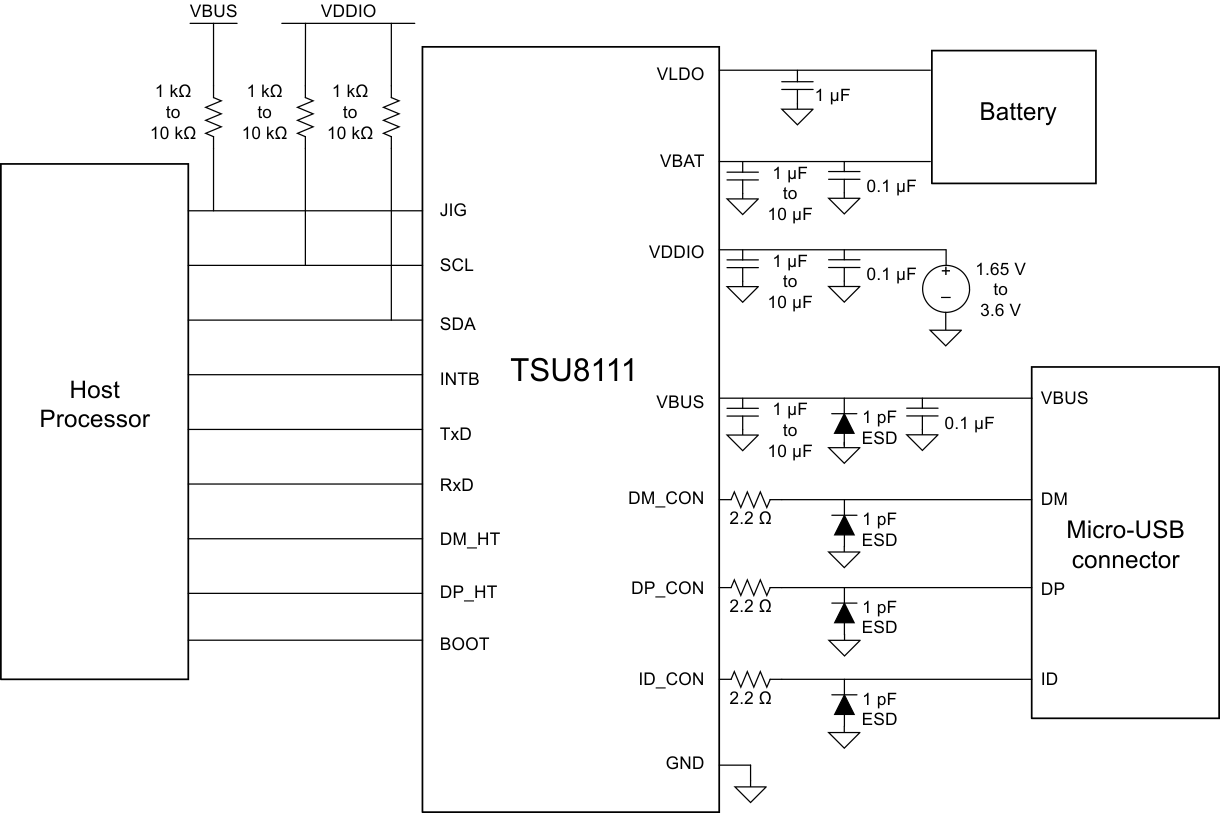 Figure 12. Interface from Host Processor to USB Connector and Battery
8.2.1 Design Requirements
For this design example, use the parameters listed in Table 24.
Table 24. Design Parameters
| DESIGN PARAMETER | EXAMPLE VALUE |
|---|---|
| VBAT | 3 V to 4.4 V |
| VBUS | 4 V to 6.5 V |
| VDDIO | 1.65 V to 3.6 V |
8.2.2 Detailed Design Procedure
To begin the design process, determine the following:
- Desired ESD protection on micro-USB signal lines
- Addition of optional 1-pF ESD diodes on the USB lines protects against ±8-kV IEC-61000-4-2 contact discharge. The optional 2.2-Ω resistors provide additional protection for the internal circuitry near the USB inputs.
- Output current on LDO
- Use the charging specifications for the Li-Ion or Li-Polymer battery to determine the desired output current register setting for the TSU8111 LDO.
8.2.3 Application Curves
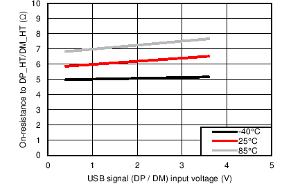 Figure 13. USB Signal vs On-resistance