ZHCSAE4A September 2012 – August 2014 TSU8111
PRODUCTION DATA.
- 1 特性
- 2 应用范围
- 3 说明
- 4 修订历史记录
- 5 Pin Configuration and Functions
- 6 Specifications
-
7 Detailed Description
- 7.1 Overview
- 7.2 Functional Block Diagram
- 7.3 Feature Description
- 7.4 Device Functional Modes
- 7.5 Programming
- 7.6
Register Map
- 7.6.1 Device ID (01h) Register Field Descriptions
- 7.6.2 Control (02h) Register Field Descriptions
- 7.6.3 Interrupt 1 (03h) Register Field Descriptions
- 7.6.4 Interrupt 2 (04h) Register Field Descriptions
- 7.6.5 Interrupt Mask 1 (05h) Register Field Descriptions
- 7.6.6 Interrupt Mask 2 (06h) Register Field Descriptions
- 7.6.7 ADC (07h) Register Field Descriptions
- 7.6.8 Timing Set 1 (08h) Register Field Descriptions
- 7.6.9 Timing Set 2 (09h) Register Field Descriptions
- 7.6.10 Device Type 1 (0Ah) Register Field Descriptions
- 7.6.11 Device Type 2 (0Bh) Register Field Descriptions
- 7.6.12 Button 1 (0Ch) Register Field Descriptions
- 7.6.13 Button 2 (0Dh) Register Field Descriptions
- 7.6.14 Manual SW 1 (13h) Register Field Descriptions
- 7.6.15 Manual SW 2 (14h) Register Field Descriptions
- 7.6.16 Reset (1Bh) Register Field Descriptions
- 7.6.17 Charger control 1 (20h) Register Field Descriptions
- 7.6.18 Charger control 2 (21h) Register Field Descriptions
- 7.6.19 Battery Charger Control 3 (22h) Register Field Descriptions
- 7.6.20 Charger Interrupt (24h) Register Field Descriptions
- 7.6.21 Charger Interrupt Mask (25h) Register Field Descriptions
- 7.6.22 Charger Status (26h) Register Field Descriptions
- 8 Application and Implementation
- 9 Power Supply Recommendations
- 10Layout
- 11器件和文档支持
- 12机械封装和可订购信息
5 Pin Configuration and Functions
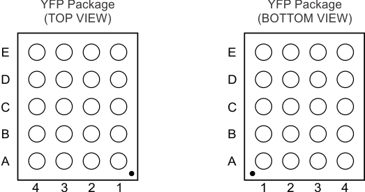
Pin Functions
| PIN | I/O | DESCRIPTION | |
|---|---|---|---|
| NAME | NO. | ||
| BOOT | B2 | O | BOOT mode used for factory test modes. Push-pull output (active high) |
| DM_CON | C4 | I/O | USB DM connected to USB receptacle |
| DM_HT | D1 | I/O | USB DM on device side |
| DP_CON | D4 | I/O | USB DP connected to USB receptacle |
| DP_HT | E1 | I/O | USB DP on device side |
| GND | A2, D3 | — | Ground |
| ID_CON | E4 | I/O | USB ID connected to USB receptacle |
| INTB | C3 | O | Interrupt to host. Push-pull output (active high) |
| JIG | C2 | O | JIG detection used for factory test modes. Open-drain output (active low) |
| RxD | C1 | I/O | UART Rx – capable of passing USB 2.0 HS signals |
| SCL | E3 | I | I2C clock |
| SDA | E2 | I/O | I2C data |
| TxD | B1 | I/O | UART Tx – capable of passing USB 2.0 HS signals |
| VBAT | A3, B3 | I | Supply voltage from battery |
| VBUS | A4, B4 | I | Supply voltage from micro-USB connector. Charger is enabled when this supply is present. |
| VDDIO | D2 | I | I2C and interrupt interface logic supply voltage |
| VLDO | A1 | O | Low dropout regulator (LDO) charger output |