SCDS241B May 2008 – December 2016 TS5A9411
PRODUCTION DATA.
- 1 Features
- 2 Applications
- 3 Description
- 4 Revision History
- 5 Pin Configuration and Functions
- 6 Specifications
- 7 Parameter Measurement Information
- 8 Detailed Description
- 9 Application and Implementation
- 10Power Supply Recommendations
- 11Layout
- 12Device and Documentation Support
- 13Mechanical, Packaging, and Orderable Information
8 Detailed Description
8.1 Overview
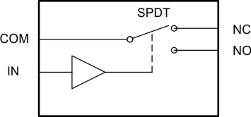
The TS5A9411 device is a 1:2 or single-pole-double-throw (SPDT) solid-state analog switch. The TS5A9411, like all analog switches, is bidirectional. When powered on, each COM pin is connected to the NC pin or NO pin depending on the status of the IN pin. If IN is low, COM is connected to NC. If IN is high, COM is connected to NO. The TS5A9411 is a break-before-make switch. This means that during switching, a connection is broken before a new connection is established. The NC and NO pins are never connected to each other.
8.2 Functional Block Diagram

8.3 Feature Description
The low ON-state resistance, ON-state resistance matching, and charge injection in the TS5A9411 make this switch an excellent choice for analog signals that require minimal distortion. The 2.25-V to 5.5-V operation allows compatibility with more voltage nodes, and the bidirectional I/Os can pass analog signals from 0 V to VCC with low distortion.
8.4 Device Functional Modes
Table 1 lists the functional modes of the TS5A9411. If IN pin is low, COM is connected to NC. If IN is high, COM is connected to NO.
Table 1. Function Table
| IN | NC TO COM, COM TO NC | NO TO COM, COM TO NO |
|---|---|---|
| L | ON | OFF |
| H | OFF | ON |