SCDS261H March 2008 – June 2017 TS5A22364
PRODUCTION DATA.
- 1 Features
- 2 Applications
- 3 Description
- 4 Revision History
- 5 Pin Configuration and Functions
- 6 Specifications
- 7 Parameter Measurement Information
- 8 Detailed Description
- 9 Application and Implementation
- 10Power Supply Recommendations
- 11Layout
- 12Device and Documentation Support
- 13Mechanical, Packaging, and Orderable Information
封装选项
机械数据 (封装 | 引脚)
散热焊盘机械数据 (封装 | 引脚)
- DRC|10
订购信息
9 Application and Implementation
NOTE
Information in the following applications sections is not part of the TI component specification, and TI does not warrant its accuracy or completeness. TI’s customers are responsible for determining suitability of components for their purposes. Customers should validate and test their design implementation to confirm system functionality.
9.1 Application Information
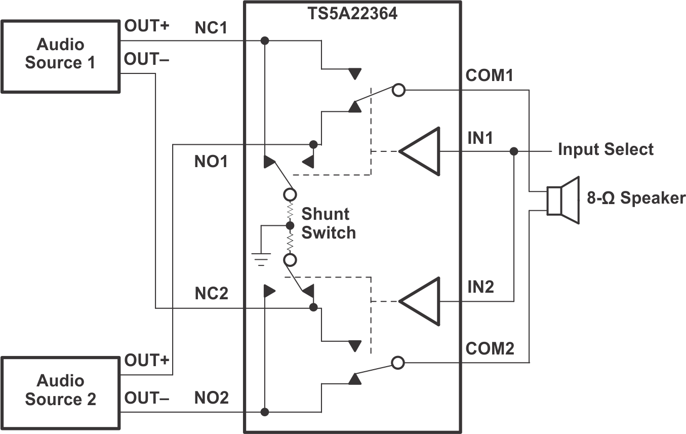
The shunt resistors on the TS5A22364 automatically discharge any capacitance at the NC or NO terminals when they are not connected to COM. This reduces audible click-and-pop sounds that occur when switching between audio sources. Audible clicks and pops are caused when a step DC voltage is switched into the speaker. By automatically discharging the side that is not connected, any residual DC voltage is removed, thereby reducing the clicks and pops.
9.2 Typical Application
The shunt resistors on the TS5A22364 are designed to automatically discharge any residual charge at the NC or NO terminals when they are not connected to COM. This reduces audible click-and-pop sounds that occur when switching between audio sources. Audible clicks and pops are caused when a step DC voltage is switched into the speaker. By automatically discharging the side that is not used for the signal path, any residual charge voltage is discharged to ground, thereby reducing the clicks and pops. The amount of power that the shunt switch can discharge from the inactive signal path is limited by the shunt resistors (Rsh) power dissipation. TI recommends that during operation, the current through the shunt path should be limited to ±10 mA.
 Figure 24. Shunt Switch (TS5A22364)
9.2.1 Design Requirements
Tie the digitally controlled inputs select pins IN1 and IN2 to VCC or GND to avoid unwanted switch states and high current consumption that could result if the logic control pins are left floating.
9.2.2 Detailed Design Procedure
Select the appropriate supply voltage to cover the entire voltage swing of the signal passing through the switch because the TS5A22364 operates from a single 2.3-V to 5.5-V supply and the input and output signal swing of the device is dependant of the supply voltage, VCC. The device will pass signals as high as VCC and as low as VCC – 5.5 V. Use Table 1 as a guide for selecting supply voltage based on the signal passing through the ON-state switch path.
Ensure that the device is powered up with a valid supply voltage on VCC before a voltage can be applied to the signal paths NC and NO.
9.2.3 Application Curve
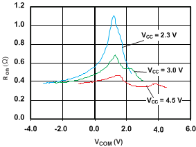
 Figure 25. Ron vs VCOM