ZHCS023D January 2010 – October 2022 TS3A27518E-Q1
PRODUCTION DATA
- 1 特性
- 2 应用
- 3 说明
- 4 Revision History
- 5 Pin Configuration and Functions
- 6 Specifications
- 7 Parameter Measurement Information
- 8 Detailed Description
- 9 Application and Implementation
- 10Power Supply Recommendations
- 11Layout
- 12Device and Documentation Support
- 13Mechanical, Packaging, and Orderable Information
封装选项
机械数据 (封装 | 引脚)
散热焊盘机械数据 (封装 | 引脚)
- RTW|24
订购信息
7 Parameter Measurement Information
Table 7-1 Parameter Description
| SYMBOL | DESCRIPTION |
|---|---|
| VCOM | Voltage at COM |
| VNC | Voltage at NC |
| VNO | Voltage at NO |
| ron | Resistance between COM and NC or NO ports when the channel is ON |
| Δron | Difference of ron between channels in a specific device |
| ron(flat) | Difference between the maximum and minimum value of ron in a channel over the specified range of conditions |
| INC(OFF) | Leakage current measured at the NC port, with the corresponding channel (NC to COM) in the OFF state |
| INC(ON) | Leakage current measured at the NC port, with the corresponding channel (NC to COM) in the ON state and the output (COM) open |
| INO(OFF) | Leakage current measured at the NO port, with the corresponding channel (NO to COM) in the OFF state |
| INO(ON) | Leakage current measured at the NO port, with the corresponding channel (NO to COM) in the ON state and the output (COM) open |
| ICOM(OFF) | Leakage current measured at the COM port, with the corresponding channel (COM to NC or NO) in the OFF state |
| ICOM(ON) | Leakage current measured at the COM port, with the corresponding channel (COM to NC or NO) in the ON state and the output (NC or NO) open |
| VIH | Minimum input voltage for logic high for the control input (IN, EN) |
| VIL | Maximum input voltage for logic low for the control input (IN, EN) |
| VI | Voltage at the control input (IN, EN) |
| IIH, IIL | Leakage current measured at the control input (IN, EN) |
| tON | Turn-on time for the switch. This parameter is measured under the specified range of conditions and by the propagation delay between the digital control (IN) signal and analog output NC or NO) signal when the switch is turning ON. |
| tOFF | Turn-off time for the switch. This parameter is measured under the specified range of conditions and by the propagation delay between the digital control (IN) signal and analog output (NC or NO) signal when the switch is turning OFF. |
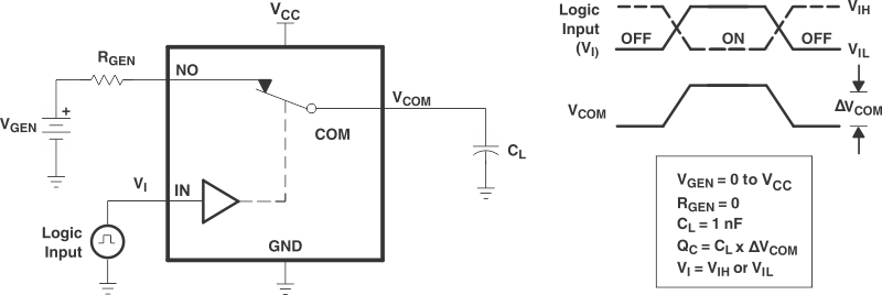
| QC | Charge injection is a measurement of unwanted signal coupling from the control (IN) input to the analog (NC or NO) output. This is measured in coulomb (C) and measured by the total charge induced due to switching of the control input. Charge injection, QC = CL × ΔVCOM, CL is the load capacitance and ΔVCOM is the change in analog output voltage. |
| CNC(OFF) | Capacitance at the NC port when the corresponding channel (NC to COM) is OFF |
| CNC(ON) | Capacitance at the NC port when the corresponding channel (NC to COM) is ON |
| CNO(OFF) | Capacitance at the NC port when the corresponding channel (NO to COM) is OFF |
| CNO(ON) | Capacitance at the NC port when the corresponding channel (NO to COM) is ON |
| CCOM(OFF) | Capacitance at the COM port when the corresponding channel (COM to NC) is OFF |
| CCOM(ON) | Capacitance at the COM port when the corresponding channel (COM to NC) is ON |
| CI | Capacitance of control input (IN, EN) |
| OISO | OFF isolation of the switch is a measurement of OFF-state switch impedance. This is measured in dB in a specific frequency, with the corresponding channel (NC to COM) in the OFF state. |
| XTALK | Crosstalk is a measurement of unwanted signal coupling from an ON channel to an OFF channel (NC1 to NO1). Adjacent crosstalk is a measure of unwanted signal coupling from an ON channel to an adjacent ON channel (NC1 to NC2) .This is measured in a specific frequency and in dB. |
| BW | Bandwidth of the switch. This is the frequency in which the gain of an ON channel is –3 dB below the DC gain. |
| THD | Total harmonic distortion describes the signal distortion caused by the analog switch. This is defined as the ratio of root mean square (RMS) value of the second, third, and higher harmonic to the absolute magnitude of the fundamental harmonic. |
| I+ | Static power-supply current with the control (IN) pin at V+ or GND |
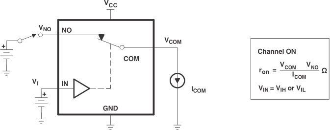 Figure 7-1 ON-state
Resistance (rON)
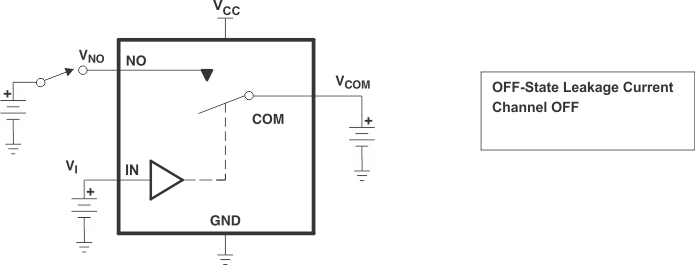 Figure 7-2 OFF-State
Leakage Current (ICOM(OFF), INC(OFF),
ICOM(PWROFF), INC(PWROFF))
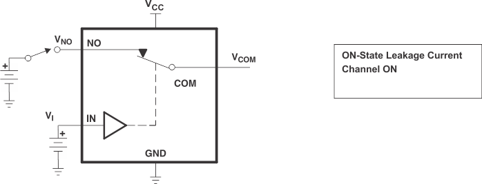 Figure 7-3 ON-State
Leakage Current (ICOM(ON), INC(ON))
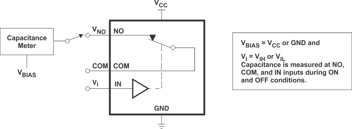 Figure 7-4 Capacitance (CI, CCOM(OFF), CCOM(ON),
CNC(OFF), CNC(ON))
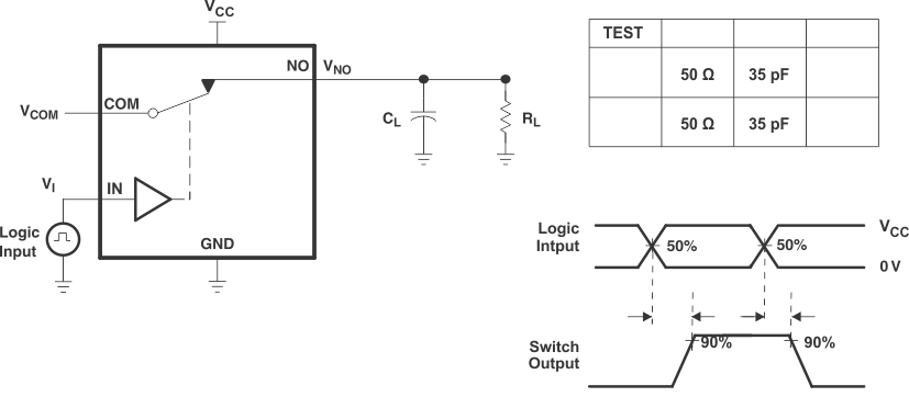
A. All input pulses are supplied by
generators having the following characteristics: PRR ≤ 10 MHz, ZO =
50 Ω, tr < 5 ns, tf < 5 ns.
B. CL includes probe and
jig capacitance.
Figure 7-5 Turn-On
(tON) and Turn-Off Time (tOFF)
A. CL includes probe and
jig capacitance.
B. All input pulses are supplied by
generators having the following characteristics: PRR ≤ 10 MHz, ZO =
50 Ω, tr < 5 ns, tf < 5 ns.
Figure 7-6 Break-Before-Make Time (tBBM)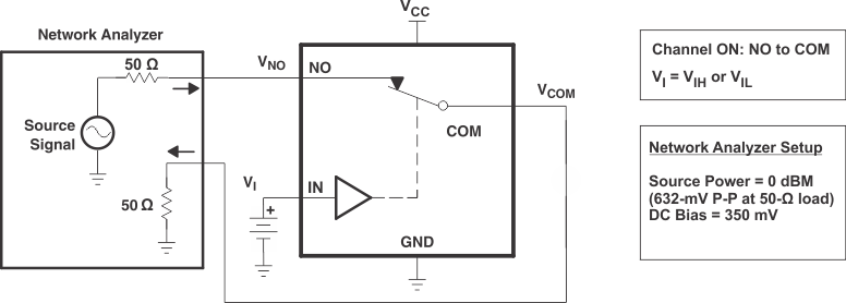 Figure 7-7 Bandwidth
(BW)
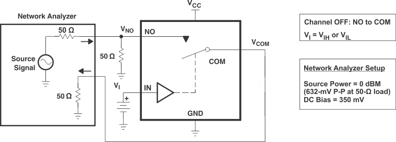 Figure 7-8 OFF
Isolation (OISO)
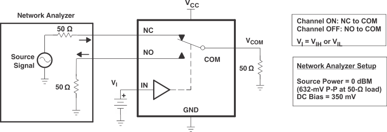 Figure 7-9 Crosstalk
(XTALK)
A. All input pulses are supplied by
generators having the following characteristics: PRR ≤ 10 MHz, ZO =
50 Ω, tr < 5 ns, tf < 5 ns.
B. CL includes probe and
jig capacitance.
Figure 7-10 Charge
Injection (QC)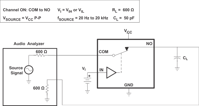
A. CL includes probe and
jig capacitance.
Figure 7-11 Total
Harmonic Distortion (THD)