SLLS850D January 2008 – March 2017 TRS3253E
PRODUCTION DATA.
- 1 Features
- 2 Applications
- 3 Description
- 4 Revision History
- 5 Pin Configuration and Functions
-
6 Specifications
- 6.1 Absolute Maximum Ratings
- 6.2 ESD Ratings
- 6.3 Recommended Operating Conditions
- 6.4 Thermal Information
- 6.5 Electrical Characteristics—Power
- 6.6 Electrical Characteristics—Driver
- 6.7 Electrical Characteristics—Receiver
- 6.8 Electrical Characteristics—Status
- 6.9 Switching Characteristics—Driver
- 6.10 Switching Characteristics—Receiver
- 6.11 Switching Characteristics—Power and Status
- 6.12 Typical Characteristics
- 7 Parameter Measurement Information
- 8 Detailed Description
- 9 Application and Implementation
- 10Power Supply Recommendations
- 11Layout
- 12Device and Documentation Support
- 13Mechanical, Packaging, and Orderable Information
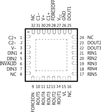
5 Pin Configuration and Functions
RSM Package
32-Pin VQFN
Top View

Power pad can be connected to GND or floating.
NC – No internal connection.
Pin Functions
| PIN | I/O | DESCRIPTION | |
|---|---|---|---|
| NAME | NO. | ||
| C1+ | 29 | — | Positive terminals of the voltage-doubler charge-pump capacitors |
| C2+ | 1 | ||
| C1– | 31 | — | Negative terminals of the voltage-doubler charge-pump capacitors |
| C2– | 2 | ||
| DIN1 | 4 | I | Driver inputs |
| DIN2 | 5 | ||
| DIN3 | 7 | ||
| DOUT1 | 25 | O | RS-232 driver outputs |
| DOUT2 | 23 | ||
| DOUT3 | 22 | ||
| FORCEOFF | 28 | I | Auto-powerdown-plus control input |
| FORCEON | 9 | I | Auto-powerdown-plus control input |
| GND | 26 | — | Ground |
| INVALID | 6 | O | Invalid output pin. Active low when all RIN inputs are unpowered |
| NC | 8 | — | No connect pins (do not connect to these pins) |
| 16 | |||
| 24 | |||
| 32 | |||
| RIN1 | 21 | I | RS-232 receiver inputs |
| RIN2 | 20 | ||
| RIN3 | 19 | ||
| RIN4 | 18 | ||
| RIN5 | 17 | ||
| ROUT1 | 14 | O | Receiver outputs. Swing between 0 and VL |
| ROUT2 | 13 | ||
| ROUT3 | 12 | ||
| ROUT4 | 11 | ||
| ROUT5 | 10 | ||
| VCC | 27 | — | 3-V to 5.5-V supply voltage |
| VL | 15 | — | Logic-level supply. All CMOS inputs and outputs are referenced to this supply |
| V+ | 30 | O | 5.5-V supply generated by the charge pump |
| V– | 3 | O | –5.5-V supply generated by the charge pump |