ZHCSCH9 May 2014 TRF37D73
PRODUCTION DATA.
6 Specifications
6.1 Absolute Maximum Ratings
over operating free-air temperature range (unless otherwise noted) (1)| MIN | MAX | UNIT | ||
|---|---|---|---|---|
| Supply Input voltage | –0.3 | 3.6 | V | |
| Input Power | 10 | dBm | ||
| Operating virtual junction temperature range | –40 | 150 | °C | |
(1) Stresses beyond those listed under Absolute Maximum Ratings may cause permanent damage to the device. These are stress ratings only, which do not imply functional operation of the device at these or any other conditions beyond those indicated under Recommended Operating Conditions. Exposure to absolute-maximum-rated conditions for extended periods may affect device reliability.
6.2 Handling Ratings
| MIN | MAX | UNIT | |||
|---|---|---|---|---|---|
| TSTG | Storage temperature range | –65 | 150 | °C | |
| VESD | Electrostatic discharge | Human body model (HBM), per ANSI/ESDA/JEDEC JS-001, all pins(1) | –1 | 1 | kV |
| Charged device model (CDM), per JEDEC specification JESD22-C101, all pins (2) | –1 | 1 | kV | ||
(1) JEDEC document JEP155 states that 500-V HBM allows safe manufacturing with a standard ESD control process.
(2) JEDEC document JEP157 states that 250-V CDM allows safe manufacturing with a standard ESD control process.
6.3 Recommended Operating Conditions
over operating free-air temperature range (unless otherwise noted)| MIN | NOM | MAX | UNIT | ||
|---|---|---|---|---|---|
| Supply Voltage, VCC | 3 | 3.3 | 3.45 | V | |
| Operating junction temperature, TJ | –40 | 125 | °C | ||
6.4 Thermal Information
| THERMAL METRIC(1) | DSG | UNIT | |
|---|---|---|---|
| 8 PINS | |||
| RθJA | Junction-to-ambient thermal resistance | 79.3 | °C/W |
| RθJCtop | Junction-to-case (top) thermal resistance | 110 | |
| RθJB | Junction-to-board thermal resistance | 49 | |
| ψJT | Junction-to-top characterization parameter | 6 | |
| ψJB | Junction-to-board characterization parameter | 49.4 | |
| RθJCbot | Junction-to-case (bottom) thermal resistance | 19.2 | |
(1) For more information about traditional and new thermal metrics, see the IC Package Thermal Metrics application report, SPRA953.
6.5 Electrical Characteristics
VCC = 3V3, TA = 25°C, PWDN = Low, LOUT = 100 nH, C1 = C2 = 1000 pF, ZS = ZL = 50 Ω (unless otherwise noted)| PARAMETER | TEST CONDITIONS | MIN | TYP | MAX | UNIT | |
|---|---|---|---|---|---|---|
| DC PARAMETERS | ||||||
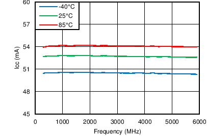
| ICC | Total supply current | 53 | 65 | mA | ||
| Power down current | PWDN = High | 125 | µA | |||
| Pdiss | Power dissipation | 0.175 | W | |||
| RF REQUENCY RANGE | ||||||
| Frequency range | 1 | 6000 | MHz | |||
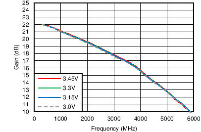
| G | Small signal gain | fRF = 400 MHz | 22 | dB | ||
| fRF = 2000 MHz | 19.5 | dB | ||||
| fRF = 3000 MHz | 18 | dB | ||||
| fRF = 4000 MHz | 15.5 | dB | ||||
| fRF = 5000 MHz | 13 | dB | ||||
| fRF = 6000 MHz | 10 | dB | ||||
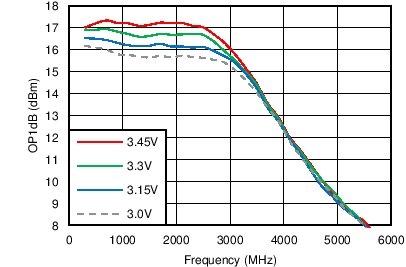
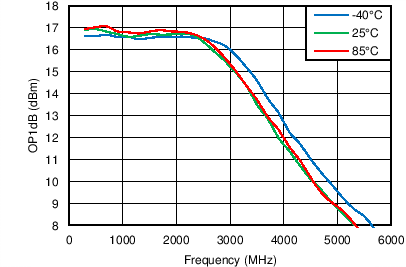
| OP1dB | Output 1dB compression point | At 2000 MHz | 16.5 | dBm | ||
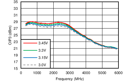
| OIP3 | Output 3rd order intercept point | At 2000 MHz, 2-tone 10 MHz apart | 27.5 | dBm | ||
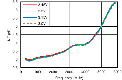
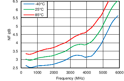
| NF | Noise figure | At 2000 MHz | 3.25 | dB | ||
| R(LI) | Input return loss | At 2000 MHz | 20 | dB | ||
| R(LO) | Output return loss | At 2000 MHz | 12 | dB | ||
| PWDN PIN | ||||||
| VIH | High level input level | 2 | V | |||
| VIL | Low level input level | 0.8 | V | |||
| IIH | High level input current | 30 | µA | |||
| IIL | Low level input current | 1 | µA | |||
6.6 Timing Requirements
| MIN | TYP | MAX | UNIT | |||
|---|---|---|---|---|---|---|
| PWDN PIN | ||||||
| tON | Turn-on Time | 50% TTL to 90% POUT | 0.6 | µs | ||
| tOFF | Turn-off Time | 50% TTL to 10% POUT | 1.4 | µs | ||
6.7 Typical Characteristics
| VCC curves | Temp = 25°C | Pin = –10 dBm |
| VCC curves | Temp = 25°C |
| VCC curves | Temp = 25°C | Pin = –10 dBm/tone |
| VCC curves | Temp = 25°C |
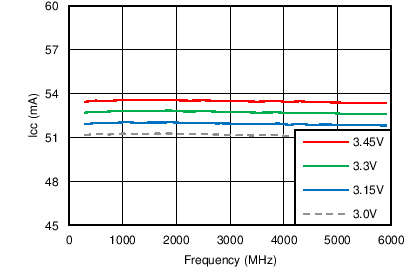
| VCC curves | Temp = 25°C |
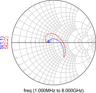
| VCC = 3.3 V | Temp = 25°C | 1 MHz to 8 GHz |
| Data Taken with EVM and Bias T, De-embedded to DUT pin | ||
3
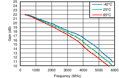
Figure 2. Gain vs Frequency
| Temp curves | VCC = 3.3 V | Pin = –10 dBm |
| Temp curves | VCC = 3.3 V |
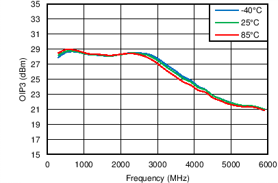
| Temp curves | VCC = 3.3 V | Pin = –10 dBm/tone |
| Temp curves | VCC = 3.3 V |
| Temp curves | VCC = 3.3 V |
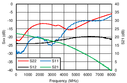
| VCC = 3.3 V | Temp = 25°C | 1 MHz to 8 GHz |
| Data Taken with EVM and Bias T, De-embedded to DUT pin | ||