ZHCSMU2B December   2020  – October 2021 TPSM5601R5H , TPSM5601R5HE

PRODUCTION DATA  

  1. 特性
  2. 应用
  3. 说明
  4. Revision History
  5. Device Comparison Table
  6. Pin Configuration and Functions
  7. Specifications
    1. 7.1 Absolute Maximum Ratings
    2. 7.2 ESD Ratings
    3. 7.3 Recommended Operating Conditions
    4. 7.4 Thermal Information
    5. 7.5 Electrical Characteristics
    6. 7.6 Typical Characteristics (VIN = 12 V)
    7. 7.7 Typical Characteristics (VIN = 24 V)
    8. 7.8 Typical Characteristics (VIN = 48 V)
    9. 7.9 Typical Characteristics (VIN = 60 V)
  8. Detailed Description
    1. 8.1 Overview
    2. 8.2 Functional Block Diagram
    3. 8.3 Feature Description
      1. 8.3.1 Adjustable Output Voltage (FB)
      2. 8.3.2 Minimum Input Capacitance
      3. 8.3.3 Minimum Output Capacitance
      4. 8.3.4 Precision Enable (EN), Undervoltage Lockout (UVLO), and Hysteresis (HYS)
      5. 8.3.5 Power Good (PGOOD)
      6. 8.3.6 Spread Spectrum Operation
      7. 8.3.7 Overcurrent Protection (OCP)
      8. 8.3.8 Thermal Shutdown
    4. 8.4 Device Functional Modes
      1. 8.4.1 Active Mode
      2. 8.4.2 Standby Mode
      3. 8.4.3 Shutdown Mode
  9. Applications and Implementation
    1. 9.1 Application Information
    2. 9.2 Typical Application
      1. 9.2.1 Design Requirements
      2. 9.2.2 Detailed Design Procedure
        1. 9.2.2.1 Custom Design With WEBENCH® Tools
        2. 9.2.2.2 Output Voltage Setpoint
        3. 9.2.2.3 Input Capacitors
        4. 9.2.2.4 Output Capacitor Selection
        5. 9.2.2.5 Power Good Signal
      3. 9.2.3 Application Curves
  10. 10Power Supply Recommendations
  11. 11Layout
    1. 11.1 Layout Guidelines
    2. 11.2 Layout Example
      1. 11.2.1 Theta JA versus PCB Area
      2. 11.2.2 Package Specifications
      3. 11.2.3 EMI
        1. 11.2.3.1 EMI Plots
  12. 12Device and Documentation Support
    1. 12.1 Device Support
      1. 12.1.1 第三方产品免责声明
      2. 12.1.2 Development Support
        1. 12.1.2.1 Custom Design With WEBENCH® Tools
    2. 12.2 Documentation Support
      1. 12.2.1 Related Documentation
    3. 12.3 Receiving Notification of Documentation Updates
    4. 12.4 支持资源
    5. 12.5 Trademarks
    6. 12.6 Electrostatic Discharge Caution
    7. 12.7 术语表
  13. 13Mechanical, Packaging, and Orderable Information

封装选项

机械数据 (封装 | 引脚)
散热焊盘机械数据 (封装 | 引脚)
订购信息

Output Voltage Setpoint

The output voltage of the TPSM5601R5Hx device is externally adjustable using a resistor divider. The recommended value of RFBT is 10 kΩ. The value for RFBB can be selected from Table 8-1 or calculated using Equation 2:

Equation 2. GUID-04D03BE9-8A11-4E9C-A4EB-8BD22CCE790D-low.gif

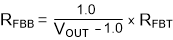
For the desired output voltage of 5 V, the formula yields a value of 2.5 kΩ. Choose the closest available standard value of 2.49 kΩ for RFBB.