ZHCSC40E February 2014 – May 2018 TPS92630-Q1
PRODUCTION DATA.
- 1 特性
- 2 应用
- 3 说明
- 4 修订历史记录
- 5 说明 (续)
- 6 Pin Configuration and Functions
- 7 Specifications
- 8 Parameter Measurement Information
- 9 Detailed Description
- 10Applications and Implementation
- 11Power Supply Recommendations
- 12Layout
- 13器件和文档支持
- 14机械、封装和可订购信息
9.3.6 Thermal Foldback
The TPS92630-Q1 device integrates thermal shutdown protection to prevent the device from overheating. In addition, to prevent LEDs from flickering because of rapid thermal changes, the device includes a programmable thermal current-foldback feature to reduce power dissipation at high junction temperatures.
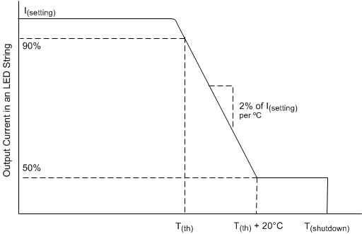
The TPS92630-Q1 device reduces the LED current as the silicon junction temperature of the TPS92630-Q1 device increases (see Figure 23). By mounting the TPS92630-Q1 device on the same thermal substrate as the LEDs, use of this feature can also limit the dissipation of the LEDs. As the junction temperature of the TPS92630-Q1 device increases, the device reduces the regulated current, reducing the dissipated power in the TPS92630-Q1 device and in the LEDs. The current reduction is from the 100% level at typically 2% of I(setting) per ºC until the point at which the current drops to 50% of the full value.
 Figure 23. Thermal Foldback
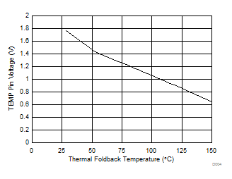
 Above this temperature, the current continues to decrease at a lower rate until the temperature reaches the overtemperature shutdown threshold temperature, T(shutdown). Changing the voltage on the TEMP pin adjusts the temperature at which the current reduction begins. With TEMP floating, the definition of thermal monitor activation temperature, T(th), is the temperature at which the current reduction begins. The specification of T(th) in the characteristics table is at the 90% current level. T(th) increases as the voltage at the TEMP pin, V(TEMP), declines and is defined as approximately:
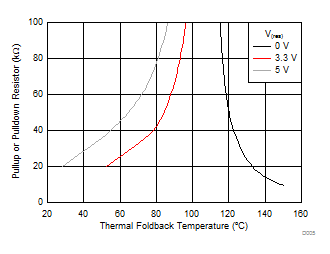
A resistor connected between TEMP and GND reduces V(TEMP) and increases T(th). A resistor connected between TEMP and a reference supply greater than 1 V increases V(TEMP) and reduces T(th).
Figure 25 shows how the nominal value of the thermal-monitor activation temperature varies with the voltage at TEMP and with either a pulldown resistor to GND or with a pullup resistor to 3.3 V or 5 V.
In extreme cases, if the junction temperature exceeds the overtemperature limit, T(shutdown), the device disables all channels. Temperature monitoring continues, and channel reactivation occurs when the temperature drops below the threshold provided by the specified hysteresis.
Note the possibility of the TPS92630-Q1 device transitioning rapidly between thermal shutdown and normal operation. This can happen if the thermal mass attached to the exposed thermal pad is small and T(th) is increased to close to the shutdown temperature. The period of oscillation depends on T(th), the dissipated power, the thermal mass of any heatsink present, and the ambient temperature.

