ZHCSD16A October   2014  – November 2014 TPS8268090 , TPS8268105 , TPS8268150

PRODUCTION DATA.  

  1. 特性
  2. 应用
  3. 说明
  4. 修订历史记录
  5. Device Comparison Table
  6. Pin Configuration and Functions
  7. Specifications
    1. 7.1 Absolute Maximum Ratings
    2. 7.2 Handling Ratings
    3. 7.3 Recommended Operating Conditions
    4. 7.4 Thermal Information
    5. 7.5 Electrical Characteristics
    6. 7.6 Typical Characteristics
  8. Parameter Measurement Information
    1. 8.1 Schematic
  9. Detailed Description
    1. 9.1 Overview
    2. 9.2 Functional Block Diagram
    3. 9.3 Feature Description
      1. 9.3.1 Soft Start
      2. 9.3.2 Undervoltage Lockout
      3. 9.3.3 Short-Circuit Protection
      4. 9.3.4 Thermal Shutdown
      5. 9.3.5 Enable
      6. 9.3.6 MODE Pin
    4. 9.4 Device Functional Modes
      1. 9.4.1 Spread Spectrum, PWM Frequency Dithering
  10. 10Application and Implementation
    1. 10.1 Application Information
    2. 10.2 Typical Application
      1. 10.2.1 Design Requirements
      2. 10.2.2 Detailed Design Procedure
        1. 10.2.2.1 Input Capacitor Selection
        2. 10.2.2.2 Output Capacitor Selection
      3. 10.2.3 Application Curves
  11. 11Power Supply Recommendations
  12. 12Layout
    1. 12.1 Layout Guidelines
    2. 12.2 Layout Example
    3. 12.3 Surface Mount Information
    4. 12.4 Thermal and Reliability Information
  13. 13器件和文档支持
    1. 13.1 文档支持
      1. 13.1.1 参考书目
    2. 13.2 相关链接
    3. 13.3 商标
    4. 13.4 静电放电警告
    5. 13.5 术语表
  14. 14机械封装和可订购信息
    1. 14.1 封装概要
    2. 14.2 MicroSiP™ DC/DC 模块封装尺寸

封装选项

机械数据 (封装 | 引脚)
散热焊盘机械数据 (封装 | 引脚)
订购信息

6 Pin Configuration and Functions
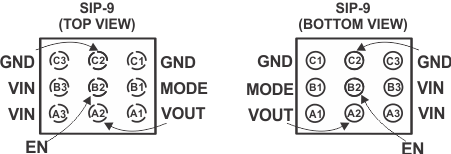
po_TPS826x_8x.gif

Pin Functions

PIN I/O DESCRIPTION
NAME NO.
VOUT A1, A2 O Power output pin. Apply output load between this pin and GND.
VIN A3, B3 I Supply voltage connection
EN B2 I This is the enable pin of the device. Connecting this pin low forces the device into shutdown mode. Pulling this pin high enables the device. This pin must not be left floating and must be terminated.
MODE B1 I This pin must be tied to the input supply voltage VIN.
GND C1, C2, C3 Ground pin.