ZHCSD16A October 2014 – November 2014 TPS8268090 , TPS8268105 , TPS8268150
PRODUCTION DATA.
10 Application and Implementation
NOTE
Information in the following applications sections is not part of the TI component specification, and TI does not warrant its accuracy or completeness. TI’s customers are responsible for determining suitability of components for their purposes. Customers should validate and test their design implementation to confirm system functionality.
10.1 Application Information
The TPS8268x device is a complete DC/DC step-down power supply optimized for small solution size. Included in the package are the switching regulator, inductor and input/output capacitors. Integration of passive components enables a tiny solution size of only 6.7mm2.
10.2 Typical Application
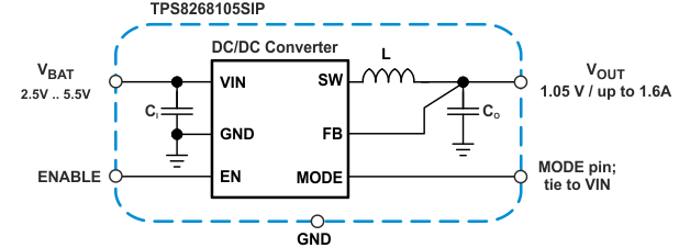 Figure 15. Typical Application Schematic
10.2.1 Design Requirements
Figure 15 shows the schematic of the typical application. The following design guidelines provide all information to operate the device within the recommended operating conditions.
10.2.2 Detailed Design Procedure
The TPS8268x allows the design of a complete power supply with no additional external components. The input capacitance can be increased in case the source impedance is large or if there are high load transients expected at the output. The dc bias effect of the input and output capacitors must be taken into account and the total capacitance on the output must not exceed the value given in the recommended operating conditions.
10.2.2.1 Input Capacitor Selection
Because the nature of the buck converter has a pulsating input current, a low ESR input capacitor is required.
For most applications, the input capacitor that is integrated into the TPS8268x is sufficient. If the application exhibits a noisy or erratic switching frequency, experiment with additional input ceramic capacitance to find a remedy.
The TPS8268x uses a tiny ceramic input capacitor. When a ceramic capacitor is combined with trace or cable inductance, such as from a wall adapter, a load step at the output can induce ringing at the VIN pin. This ringing can couple to the output and be mistaken as loop instability or can even damage the part. In this circumstance, additional "bulk" capacitance, such as electrolytic or tantalum, should be placed between the input of the converter and the power source lead to reduce ringing that can occur between the inductance of the power source leads and CI.
10.2.2.2 Output Capacitor Selection
The advanced fast-response voltage mode control scheme of the TPS8268x allows the use of tiny ceramic output capacitors. Ceramic capacitors with low ESR values have the lowest output voltage ripple and are recommended. For most applications, the output capacitor integrated in the TPS8268x is sufficient. An additional output capacitor may be used for the purpose of improving AC voltage accuracy during large load transients.
To further reduce the voltage drop during load transients, additional external output capacitance up to 30µF can be added. A low ESR multilayer ceramic capacitor (MLCC) is suitable for most applications. The total effective output capacitance must remain below 30µF.
As the device operates in PWM mode, the overall output voltage ripple is the sum of the voltage step that is caused by the output capacitor´s ESL and the ripple current that flows through the output capacitor´s impedance.
Because the damping factor in the output path is directly related to several resistive parameters (e.g. inductor DCR, power-stage rDS(on), PCB DC resistance, load switches rDS(on) …) that are temperature dependant, the converter´s small and large signal behavior should be checked over the input voltage range, load current range and temperature range.
The easiest test is to evaluate, directly at the converter’s output, the following items:
- efficiency
- load transient response
- output voltage ripple
During the recovery time from a load transient, the output voltage can be monitored for settling time, overshoot or ringing that helps judge the converter’s stability. Without any ringing, the loop typically has more than 45° of phase margin.
10.2.3 Application Curves
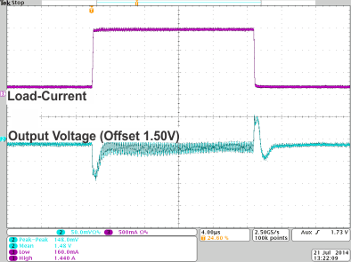 Figure 16. Load Transient Response for TPS8268150
 (Vout = 1.5V, Iout = 160mA to 1.44A to 160mA, Vin = 5V)
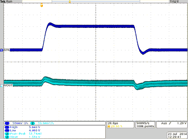 Figure 17. Line Transient Response for TPS8268150
 (Vout = 1.5V, Iout = 800mA, Vin = 4V to 5V to 4V)
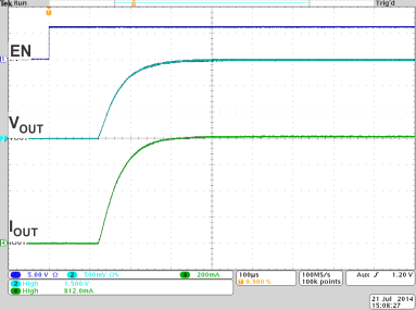 Figure 18. Startup for TPS8268150
 (Vin = 5V, Vout = 1.5V)
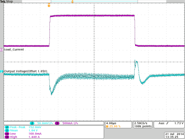 Figure 20. Load Transient Response for TPS8268105
 (Vout = 1.05V, Iout = 160mA to 1.44A to 160mA, Vin = 5V)
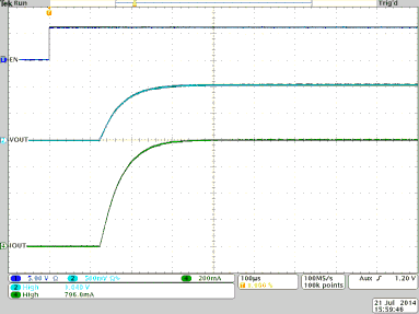 Figure 22. Startup for TPS8268105
 (Vin = 5V, Vout = 1.05V)
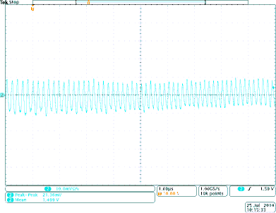 Figure 19. Output Voltage Ripple for TPS8268150
 (Vin = 5V, Vout = 1.5V, Iout = 900mA)
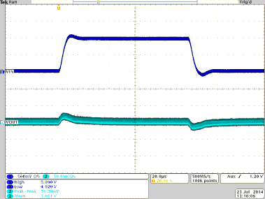 Figure 21. Line Transient Response for TPS8268105
 (Vout = 1.05V; Iout = 900mA, Vin = 4V to 5V to 4V)
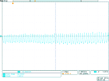 Figure 23. Output Voltage Ripple for TPS8268105
 (Vin = 5V, Vout = 1.05V, Iout = 900mA)
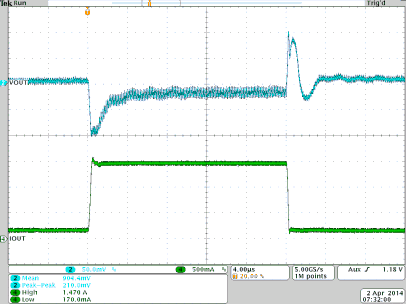 Figure 24. Load Transient Response for TPS8268090
 (Vout = 0.9V, Iout = 170mA to 1.47A to 170mA, Vin = 5V)
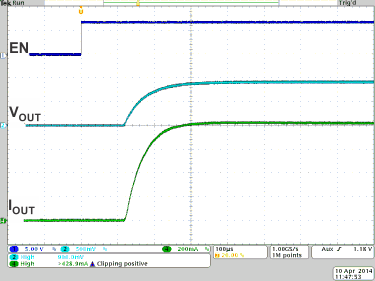 Figure 26. Startup for TPS8268090
 (Vin = 5V, Vout = 0.9V)
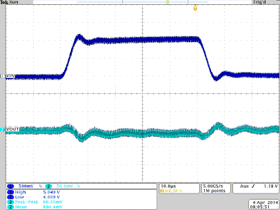 Figure 25. Line Transient Response for TPS8268090
 (Vout = 0.90V; Iout = 900mA, Vin = 4V to 5V to 4V)
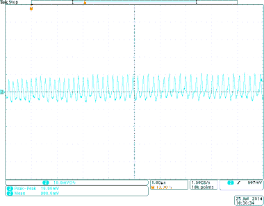 Figure 27. Output Voltage Ripple for TPS8268090
(Vin = 5V, Vout = 0.9V, Iout = 900mA)