ZHCSMP6A November 2020 – December 2021 TPS7H4010-SEP
PRODUCTION DATA
- 1 特性
- 2 应用
- 3 说明
- 4 Revision History
- 5 Pin Configuration and Functions
- 6 Specifications
-
7 Detailed Description
- 7.1 Overview
- 7.2 Functional Block Diagram
- 7.3
Feature Description
- 7.3.1 Synchronous Step-Down Regulator
- 7.3.2 Auto Mode and FPWM Mode
- 7.3.3 Fixed-Frequency Peak Current-Mode Control
- 7.3.4 Adjustable Output Voltage
- 7.3.5 Enable and UVLO
- 7.3.6 Internal LDO, VCC_UVLO, and BIAS Input
- 7.3.7 Soft Start and Voltage Tracking
- 7.3.8 Adjustable Switching Frequency
- 7.3.9 Frequency Synchronization and Mode Setting
- 7.3.10 Internal Compensation and CFF
- 7.3.11 Bootstrap Capacitor and VBOOT-UVLO
- 7.3.12 Power-Good and Overvoltage Protection
- 7.3.13 Overcurrent and Short-Circuit Protection
- 7.3.14 Thermal Shutdown
- 7.4 Device Functional Modes
-
8 Application and Implementation
- 8.1 Application Information
- 8.2
Typical Application
- 8.2.1 Design Requirements
- 8.2.2
Detailed Design Procedure
- 8.2.2.1 Output Voltage Setpoint
- 8.2.2.2 Switching Frequency
- 8.2.2.3 Input Capacitors
- 8.2.2.4 Inductor Selection
- 8.2.2.5 Output Capacitor Selection
- 8.2.2.6 Feed-Forward Capacitor
- 8.2.2.7 Bootstrap Capacitors
- 8.2.2.8 VCC Capacitor
- 8.2.2.9 BIAS
- 8.2.2.10 Soft Start
- 8.2.2.11 Undervoltage Lockout Setpoint
- 8.2.2.12 PGOOD
- 8.2.3 Application Curves
- 9 Power Supply Recommendations
- 10Layout
- 11Device and Documentation Support
- 12Mechanical, Packaging, and Orderable Information
封装选项
请参考 PDF 数据表获取器件具体的封装图。
机械数据 (封装 | 引脚)
- RNP|30
- KGD|0
散热焊盘机械数据 (封装 | 引脚)
- RNP|30
订购信息
7.3.3 Fixed-Frequency Peak Current-Mode Control
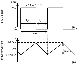
The TPS7H4010-SEP synchronous switched mode voltage regulator employs fixed frequency peak current mode control with advanced features. The fixed switching frequency is controlled by an internal clock. To get accurate DC load regulation, a voltage feedback loop is implemented to generate peak current command. The HS switch is turned on at the rising edge of the clock. As shown in Figure 7-3, during the HS switch on-time tON, the SW pin voltage VSW swings up to approximately VIN, and the inductor current IL increases with a linear slope. The HS switch is turned off when the inductor current reaches the peak current command. During the HS switch off-time tOFF, the LS switch is turned on. Inductor current discharges through the LS switch, which forces the VSW to swing below ground by the voltage drop across the LS switch. The LS switch is turned off at the next clock cycle, before the HS switch is turned on. The regulation loop adjusts the peak current command to maintain a constant output voltage.
 Figure 7-3 SW Voltage and Inductor Current Waveforms in CCM
Duty cycle D is defined by the on-time of the HS switch over the switching period:
where
- TSW = 1 / fSW is the switching period
In an ideal buck converter, where losses are ignored, D is proportional to the output voltage and inverse proportional to the input voltage: D = VOUT / VIN.
When the TPS7H4010-SEP is set to operate in auto mode, the LS switch is turned off when its current reaches zero ampere before the next clock cycle comes. Both HS switch and LS switch are off before the HS switch is turned on at the next clock cycle.