ZHCSEJ1 December 2015 TPS7H3301-SP
PRODUCTION DATA.
- 1 特性
- 2 应用
- 3 说明
- 4 修订历史记录
- 5 说明 (续)
- 6 Pin Configuration and Functions
- 7 Specifications
- 8 Detailed Description
-
9 Application and Implementation
- 9.1 Application Information
- 9.2
Typical Application
- 9.2.1 Design Requirements
- 9.2.2
Detailed Design Procedure
- 9.2.2.1 VIN/VDD Capacitor
- 9.2.2.2 VLDO Input Capacitor
- 9.2.2.3 VTT Output Capacitor
- 9.2.2.4 VTTSNS Connection
- 9.2.2.5 Low VIN Applications
- 9.2.2.6 S3 and Pseudo-S5 Support
- 9.2.2.7 Tracking Startup and Shutdown
- 9.2.2.8 Output Tolerance Consideration for VTT DIMM Applications
- 9.2.2.9 LDO Design Guidelines
- 9.2.3 Application Curve
- 10Power Supply Recommendations
- 11Layout
- 12器件和文档支持
- 13机械、封装和可订购信息
11 Layout
11.1 Layout Guidelines
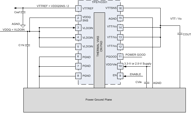
Consider the following points before starting the TPS7H3301-SP layout design.
- The input bypass capacitor for VLDOIN should be placed as close as possible to the pin with short and wide connections.
- The output capacitor for VO/VTT should be placed close to the pin with short and wide connection in order to avoid additional ESR and/or ESL trace inductance.
- VOSNS should be connected to the positive node of VO/VTT output capacitors as a separate trace from the high current power line. This configuration is strongly recommended to avoid additional ESR and/or ESL. If sensing the voltage at the point of the load is required, it is recommended to attach the output capacitor or capacitors at that point. Also, it is recommended to minimize any additional ESR and/or ESL of ground trace between the GND pin and the output capacitor or capacitors.
- Consider adding low-pass filter at VOSNS if the ESR of the VO/VTT output capacitor or capacitors is larger than 2 mΩ.
- VDDQSNS can be connected separately from VLDOIN. Remember that this sensing potential is the reference voltage of VTTREF. Avoid any noise-generating lines.
- The negative node of the VO/VTT output capacitor or capacitors and the VTTREF capacitor should be tied together by avoiding common impedance to the high current path of the VO/VTT source/sink current.
- The GND and PGND pins should be connected to the thermal land underneath the die pad with multiple vias connecting to the internal system ground planes (for better result, use at least two internal ground planes). Use as many vias as possible to reduce the impedance between PGND/GND and the system ground plane. Also, place bulk caps close to the DIMM load point, route the VOSNS to the DIMM load sense point.
- In order to effectively remove heat from the package, properly prepare the thermal land. Apply solder directly to the package’s thermal pad. The wide traces of the component and the side copper connected to the thermal land pad help to dissipate heat. Numerous vias 0.33 mm in diameter connected from the thermal land to the internal/solder side ground plane or planes should also be used to help dissipation.
11.2 Layout Example
 Figure 31. Layout Recommendation
11.3 Thermal Considerations
Because the TPS7H3301-SP is a linear regulator, the VO current flows in both source and sink directions, thereby dissipating power from the device. When the device is sourcing current, the voltage difference between VLDOIN and VO times IO (IIO ) current becomes the power dissipation as shown in Equation 2.

In this case, if VLDOIN is connected to an alternative power supply lower than the VDDQ voltage, overall power loss can be reduced. For the sink phase, VO voltage is applied across the internal LDO regulator, and the power dissipation, PDISS_SNK can be calculated by Equation 3.

Because the device does not sink and source current at the same time and the IO current may vary rapidly with time, the actual power dissipation should be the time average of the above dissipations over the thermal relaxation duration of the system. Another source of power consumption is the current used for the internal current control circuitry from the VIN supply and the VLDOIN supply. This can be estimated as 5 mW or less during normal operating conditions. This power must be effectively dissipated from the package.
The thermal performance of an LDO depends on the printed circuit board (PCB) layout. Because the TPS7H3301-SP device is shipped unformed, only the recommended heat pad pattern is shown. Lead pad placement depends on final form factor.
To further improve the thermal performance of this device, using a larger than recommended thermal land as well as increasing the number of vias helps lower the thermal resistance from junction to heat slug. TI recommends that up to 48 (0.01 inch) thermal vias can be located under the device package.